


 It’s Only Common Sense: Marketing Isn’t Fluff, It’s Ammunition
 Driving Innovation: Mechanical and Optical Processes During Rigid-flex Production
 The Chemical Connection: Onshoring PCB Production—Daunting but Certainly Possible


A Graphene Superconductor That Plays More Than One Tune
July 18, 2019 | Berkeley LabEstimated reading time: 5 minutes
What’s thinner than a human hair but has a depth of special traits? A multitasking graphene device developed by researchers at the U.S. Department of Energy’s Lawrence Berkeley National Laboratory (Berkeley Lab). The superthin material easily switches from a superconductor that conducts electricity without losing any energy, to an insulator that resists the flow of electric current, and back again to a superconductor—all with a simple flip of a switch. Their findings were reported today in the journal Nature.
“Usually, when someone wants to study how electrons interact with each other in a superconducting quantum phase versus an insulating phase, they would need to look at different materials. With our system, you can study both the superconductivity phase and the insulating phase in one place,” said Guorui Chen, the study’s lead author and a postdoctoral researcher in the lab of Feng Wang, who led the study. Wang, a faculty scientist in Berkeley Lab’s Materials Sciences Division, is also a UC Berkeley physics professor.
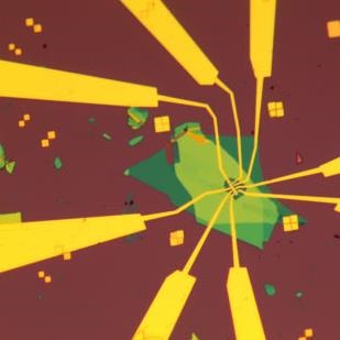
Schematic of graphene/boron nitride moire’ superlattice superconductor/insulator device: The heterostructure material is composed of three atomically thin (2D) layers of graphene (gray) sandwiched between 2D layers of boron nitride (red and blue) to form a repeating pattern called a moiré superlattice. Superconductivity is indicated by the light-green circles, which represent the hole (positive charge) sitting on each unit cell of the moiré superlattice. (Credit: Guorui Chen/Berkeley Lab)
The graphene device is composed of three atomically thin (2D) layers of graphene sandwiched between 2D layers of boron nitride to form a repeating pattern called a moiré superlattice. The material could help other scientists understand the complicated mechanics behind a phenomenon known as high-temperature superconductivity, where a material can conduct electricity without resistance at temperatures higher than expected, though still hundreds of degrees below freezing.
In a previous study, the researchers reported observing the properties of a Mott insulator in a device made of trilayer graphene. A Mott insulator is a class of material that somehow stops conducting electricity at hundreds of degrees below freezing despite classical theory predicting electrical conductivity. But it has long been believed that a Mott insulator can become superconductive by adding more electrons or positive charges to make it superconductive, Chen explained.
For the past 10 years, scientists have been studying ways to combine different 2D materials, often starting with graphene – a material known for its ability to efficiently conduct heat and electricity. Out of this body of work, it was discovered that moiré superlattices formed with graphene exhibit exotic physics such as superconductivity when the layers are aligned at just the right angle.
“So for this study we asked ourselves, ‘If our trilayer graphene system is a Mott insulator, could it also be a superconductor?’” said Chen.
Page 1 of 2
Share on:


Testimonial
"In a year when every marketing dollar mattered, I chose to keep I-Connect007 in our 2025 plan. Their commitment to high-quality, insightful content aligns with Koh Young’s values and helps readers navigate a changing industry. "
Brent Fischthal - Koh YoungSuggested Items
Sealed for Survival: Potting Electronics for the Toughest Environments
10/29/2025 | Beth Massey, MacDermid Alpha Electronics SolutionsElectronics deployed in harsh conditions face relentless threats from vibration, impact, chemical contaminants, airborne pollutants, and moisture, conditions that can quickly lead to failure without robust protection. Potting, the process of encapsulating electronics in a protective polymer, is a widely used strategy to safeguard devices from both environmental and mechanical hazards.
Driving Innovation: Mechanical and Optical Processes During Rigid-flex Production
10/28/2025 | Kurt Palmer -- Column: Driving InnovationRigid-flex printed circuit boards are a highly effective solution for placing complex circuitry in tight, three-dimensional spaces. They are now indispensable across a range of industries, from medical devices and aerospace to advanced consumer electronics, helping designers make the most efficient use of available space. However, their unique construction—combining rigid and flexible materials—presents a fundamental challenge for PCB manufacturers.
SMTAI 2025 Review: Reflecting on a Pragmatic and Forward-looking Industry
10/27/2025 | Marcy LaRont, I-Connect007Leaving the show floor on the final afternoon of SMTA International last week in Rosemont, Illinois, it was clear that the show remains a grounded, technically driven event that delivers a solid program, good networking, and an easy space to commune with industry colleagues and meet with customers.
ITW EAE Despatch Ovens Now Support ASTM 5423 Testing
10/15/2025 | ITW EAEAs the demand for high-performance electrical insulation materials continues to grow—driven by the rapid expansion of electric vehicles (EVs) and energy storage systems—thermal processing has become a critical step in material development.
Beyond Thermal Conductivity: Exploring Polymer-based TIM Strategies for High-power-density Electronics
10/13/2025 | Padmanabha Shakthivelu and Nico Bruijnis, MacDermid Alpha Electronics SolutionsAs power density and thermal loads continue to increase, effective thermal management becomes increasingly important. Rapid and efficient heat transfer from power semiconductor chip packages is essential for achieving optimal performance and ensuring long-term reliability of temperature-sensitive components. This is particularly crucial in power systems that support advanced applications such as green energy generation, electric vehicles, aerospace, and defense, along with high-speed computing for data centers and artificial intelligence (AI).