


 Global PCB Connections: Rigid-flex and Flexible PCBs—The Backbone of Modern Electronics
 Flexible Thinking: The Key to a Successful Flex Circuit Design Transfer
 Happy’s Tech Talk #29: Bend-to-Install Semi-flex FR-4


KIST Develops Technology for Creating Flexible Sensors on Topographic Surfaces
July 29, 2019 | KISTEstimated reading time: 2 minutes
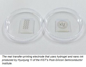
The Korea Institute of Science and Technology (KIST, president: Byung-gwon Lee) announced that Dr. Hyunjung Yi of the Post-Silicon Semiconductor Institute and her research team developed a transfer-printing technology that uses hydrogel and nano ink to easily create high-performance sensors on flexible substrates of diverse shapes and structures.
Interest in wearable devices, including smartwatches and fitness bands, is increasing rapidly. With the scope of such devices expanding from types that are worn (like clothing) to those that are attached directly to the skin, there is growing demand for technologies that allow for the production of high-performance sensors on surfaces of various shapes and types.
Transfer printing works in a way similar to that of a tattoo sticker: just as sticking the tattoo sticker onto the skin and then removing the paper section leaves the image on the skin, this process creates a structure on one surface and then transfers it onto another. The most notable advantage of this process is that it largely avoids the difficulties involved in creating devices directly on substrates that are thermally and/or chemically sensitive, which is why transfer printing is widely used for the manufacturing of flexible devices. On the other hand, the primary disadvantage of current transfer printing processes is that they can usually only be used for substrates with flat surfaces.
The KIST team overcame these limitations by developing a simple and easy transfer printing process that allows for the creation of high-performance, flexible sensors on topographic surfaces with diverse features and textures.
Using the porous and hydrophilic nature of hydrogels, the KIST team inkjet-printed an aqueous solution-based nano ink onto a hydrogel layer (which was solidified onto a topographic surface). The surfactant and water in the nano ink passed quickly through the hydrogel's porous structure, leaving only the hydrophobic nanomaterial (the particles of which are greater in length than the diameter of the holes in the hydrogel) remaining on the surface, allowing for the creation of the desired electrode pattern.
The amount of nano ink used for this printing process was very small, allowing for the rapid formation of electrodes. Moreover, the electrical performance of the electrodes was outstanding, due to the high levels of purity and uniformity of the resulting nanonetworks. Also, because of the hydrophobic nature of the nanomaterial, there was an extremely low degree of interaction between it and the hydrogel, allowing for the easy transfer of the electrodes to diverse topographic surfaces.
In particular, the KIST team developed a technology for transferring nanonetworks by employing a method that solidifies a moldable elastomeric fluid onto a hydrogel surface, enabling the easy creation of flexible electrodes even on substrates with rough surfaces. The team transferred nanoelectrodes directly onto a glove to create a modified sensor that can immediately detect finger movements. It also created a flexible, high-performance pressure sensor that can measure the pulse in the wrist.
Yi said, "The outcome of this study is a new and easy method for creating flexible, high-performance sensors on surfaces with diverse characteristics and structures. We expect that this study will be utilized in the many areas that require the application of high-performance materials onto flexible and/or non-traditional substrates, including digital healthcare, intelligent human-machine interfaces, medical engineering, and next-generation electrical materials."
Share on:


Testimonial
"Our marketing partnership with I-Connect007 is already delivering. Just a day after our press release went live, we received a direct inquiry about our updated products!"
Rachael Temple - AlltematedSuggested Items
Fresh PCB Concepts: Designing for Success at the Rigid-flex Transition Area
08/28/2025 | Team NCAB -- Column: Fresh PCB ConceptsRigid-flex PCBs come in all shapes and sizes. Manufacturers typically use fire-retardant, grade 4 (FR-4) materials in the rigid section and flexible polyimide materials in the flex region. Because of the small size, some rigid-flex PCBs, like those for hearing aid devices, are among the most challenging to manufacture. However, regardless of its size, we should not neglect the transition area between the rigid and flexible material.
Global Flexible PCB Output Expected to Surpass $20 Billion by 2025, with AI Glasses Emerging as a New Growth Driver
08/25/2025 | TPCAThe Taiwan Printed Circuit Association (TPCA) and the Industrial Technology Research Institute (ITRI) released the "2025 Global Flexible PCB Industry Outlook" in August.
Nano Silver Inks Market Forecast Report 2025-2030
08/20/2025 | Globe NewswireThe Nano Silver Inks Market is expected to grow from USD 427.415 million in 2025 to USD 836.160 million in 2030, at a CAGR of 14.36%.
Flexible Circuit Technologies to Host Free Flex Heater Webinar
08/18/2025 | Flexible Circuit TechnologiesGlobal Supplier of flexible circuits, flex design services, and assembly/box-build services, Flexible Circuit Technology will host their latest webinar, "Thermal Precision Meets Flexibility: The Technology Behind Heater Circuits" on Tuesday, August 26th, 2025 at 11 AM EDT.
Trouble in Your Tank: Metallizing Flexible Circuit Materials—Mitigating Deposit Stress
08/04/2025 | Michael Carano -- Column: Trouble in Your TankMetallizing materials, such as polyimide used for flexible circuitry and high-reliability multilayer printed wiring boards, provide a significant challenge for process engineers. Conventional electroless copper systems often require pre-treatments with hazardous chemicals or have a small process window to achieve uniform coverage without blistering. It all boils down to enhancing the adhesion of the thin film of electroless copper to these smooth surfaces.