


 Dan’s Biz Bookshelf: ‘Abundance: How We Build a Better Future’
 Trouble in Your Tank: In Complex Systems, Design Rules Aren’t Optional
 It’s Only Common Sense: The Phone Is Still Your Competitive Advantage


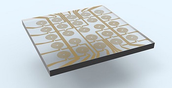
Shaping Light with a Smartlens
July 30, 2019 | ICFOEstimated reading time: 2 minutes
A team of researchers reports on a dynamically tuneable lens capable of achieving almost any complex optical function.
Camera performance on mobile devices has proven to be one of the features that most end-users aim for. The importance of optical image quality improvement, and the trend to have thinner and thinner smartphones have pushed manufactures to increase the number of cameras in order to provide phones with better zoom, low-light exposure high quality photography, portraits, to name a few. But adding additional lenses to a miniaturized optical configuration and driving light focusing with an electronic device is not as easy as it seems, particularly at small scales or in such confined spaces.
The integration of an adjustable-dynamic zoom lens in a mm-thick cell phone, in a miniaturized microscope, or at the remote end of a medical endoscope requires complex lenses that can handle the full optical spectrum and be reshaped electrically within milliseconds. Until now, a class of soft materials known as liquid crystal spatial light modulators have been the tool of choice for high-resolution light shaping, but their implementation has proven to have limits in terms of performance, bulkiness and cost.
In a study recently published in Nature Photonics, fruit of a close collaboration between Pascal Berto, Chang Liu and Gilles Tessier from the Institut de la Vision, and ICFO scientists Laurent Philippet, Johann Osmond, Adeel Afridi, Marc Montagut, and Bernat Molero, led by ICREA Prof. at ICFO Romain Quidant, the researchers demonstrate an adjustable technique to manipulate light without any mechanical movement. In this approach, coined Smartlens, a current is passed through a well-optimized micrometer-scale resistor, and the heating locally changes the optical properties of the transparent polymer plate holding the resistor. In much the same way as a mirage bends light passing through hot air to create illusions of distant lakes, this microscale hot region is able to deviate light. Within milliseconds, a simple slab of polymer can be turned into a lens and back: small, micrometer-scale smartlenses heat up and cool down quickly and with minimal power consumption. They can even be fabricated in arrays, and the authors show that several objects located at very different distances can be brought into focus within the same image by activating the Smartlenses located in front of each of them, even if the scene is in colours.
By modelling the diffusion of heat and the propagation of light and using algorithms inspired by the laws of natural selection the authors show they can go way beyond simple lenses: a properly engineered resistor can shape light with a very high level of control and achieve a wide variety of optical functions. For instance, if the right resistor is imprinted on it, a piece of polymer could be activated or deactivated at will to generate a given “freeform” and correct specific defects in our eyesight, or the aberrations of an optical instrument.
As Prof. Romain Quidant points out, “remarkably, the Smartlens technology is cost effective and scalable, and has proven to have the potential to be applied to high-end technological systems as well as simple end-user-oriented imaging devices”. The results of this study open a new window for the development of low-cost dynamically tuneable devices that could have a high impact on current existing optical systems.
Share on:


Subscribe
Stay ahead of the technologies shaping the future of electronics with our latest newsletter, Advanced Electronics Packaging Digest. Get expert insights on advanced packaging, materials, and system-level innovation, delivered straight to your inbox.
Subscribe now to stay informed, competitive, and connected.
Suggested Items
Gregoire Outters Promoted to President of Teledyne Marine Group
04/06/2026 | TeledyneTeledyne Technologies Incorporated announced the promotion of Gregoire Outters to President of its Teledyne Marine Group.
Teledyne Strengthens Commitment to the Space Sector
04/01/2026 | BUSINESS WIRETeledyne Technologies Incorporated is excited to announce the integration of the company’s extensive portfolio of space-focused technologies and businesses, reinforcing its long-term commitment to the global space sector.
Teledyne to Supply Detectors for Lazuli Space Observatory
03/30/2026 | BUSINESS WIRETeledyne Space Imaging, part of Teledyne Technologies Incorporated has been awarded a contract by Schmidt Sciences to deliver advanced near-infrared (NIR) H4RG-10 flight focal plane arrays (FPAs) and custom electronics for integration into the Integral Field Spectrograph on the groundbreaking Lazuli Space Observatory.
New Superconducting Chip Could Enable Breakthrough Nondestructive Terahertz Imaging
03/23/2026 | University of GlasgowA tiny crystal chip which uses terahertz radiation to see clearly through a wide range of materials could find applications in healthcare, biological research, and security screening.
The Test Connection Adds Creative Electron Prime TruVision™ X-ray and CT System for Deeper Failure Analysis
03/05/2026 | TTCIThe Test Connection Inc. (TTCI), a trusted provider of electronic test and manufacturing solutions for more than 45 years, has added the Prime TruVision™ X-ray and computed tomography (CT) inspection system from Creative Electron to its engineering and analysis services.