


 Dan’s Biz Bookshelf: ‘Abundance: How We Build a Better Future’
 Trouble in Your Tank: In Complex Systems, Design Rules Aren’t Optional
 It’s Only Common Sense: The Phone Is Still Your Competitive Advantage


3D Printable 2D Materials-based Inks Show Promise to Improve Energy Storage Devices
July 31, 2019 | University of ManchesterEstimated reading time: 2 minutes
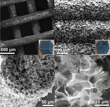
For the first time, a team of researchers, from the School of Materials and the National Graphene Institute at The the University of Manchester have formulated inks using the 2D material MXene, to produce 3D printed interdigitated electrodes.
MXene, a ‘clay-like’ two-dimensional material composed of early transition metals (such as titanium) and carbon atoms, was first developed by Drexel University. However, unlike most clays, MXene shows high electrical conductivity upon drying and is hydrophilic, allowing them to be easily dispersed in aqueous suspensions and inks.Since its isolation, graphene has opened the doors for the exploration of other two-dimensional materials, each with a range of different properties. However, in order to make use of these unique properties, 2D materials need to be efficiently integrated into devices and structures. The manufacturing approach and materials formulations are essential to realise this.
Dr Suelen Barg who led the team said: “We demonstrate that large MXene flakes spanning a few atoms thick, and water can be independently used to formulate inks with very specific viscoelastic behaviour for printing. These inks can be directly 3D printed into freestanding architectures over 20 layers tall. Due to the excellent electrical conductivity of MXene, we can employ our inks to directly 3D print current collector-free supercapacitors. The unique rheological properties combined with the sustainability of the approach open many opportunities to explore, especially in energy storage and applications requiring the functional properties of 2D MXene in customized 3D architectures.”
Wenji and Jae, PhD students at the Nano3D Lab at the University, said: “Additive manufacturing offers one possible method of building customised, multi-materials energy devices, demonstrating the capability to capture MXene’s potential for usage in energy applications. We hope this research will open avenues to fully unlock the potential of MXene for use in this field.”
The performance and application of these devices increasingly rely on the development and scalable manufacturing of innovative materials in order to enhance their performance.
Supercapacitors are devices that are able to produce massive amounts of power while using much less energy than conventional devices. There has been much work carried out on the use of 2D materials in these types of devices due to their excellent conductivity as well as having the potential to reduce the weight of the device.
Potential uses for these devices are for the automotive industry, such as in electric cars as well as for mobile phones and other electronics.
Share on:


Subscribe
Stay ahead of the technologies shaping the future of electronics with our latest newsletter, Advanced Electronics Packaging Digest. Get expert insights on advanced packaging, materials, and system-level innovation, delivered straight to your inbox.
Subscribe now to stay informed, competitive, and connected.
Suggested Items
Driving Innovation: Selecting the Right Laser Source
04/28/2026 | Simon Khesin -- Column: Driving InnovationWhen I first joined Schmoll Maschinen, I brought experience from almost every PCB process, except for laser. As I immersed myself in laser processing, I realized why it can seem so daunting to a newcomer. The complexity arises from three intersecting factors: A vast variety of laser sources: CO2, UV-nano, green-pico, UV-pico, IR-pico, and others; a diverse range of applications: Drilling, cutting, ablation, and more; and an extensive list of materials: These have vastly different absorption rates. Choosing the right machine or laser source is rarely trivial. Even for experienced engineers, answering "Which source is best?" requires examining the business's specific goals.
Institute of Circuit Technology Spring Seminar 2026: A Bright Future in Europe
04/23/2026 | Pete Starkey, I-Connect007Through the leafy lanes and spring flowers of Warwickshire and back to Meridan, the traditional centre of England, and now officially part of the Metropolitan Borough of Solihull in the county of the West Midlands, I attended the Annual General Meeting and Spring Seminar of the Institute of Circuit Technology (ICT) on April 14. Out of the AGM came notable changes in leadership at the top of the Institute: the retirement of Mat Beadel as chair and Emma Hudson as technical director. Effective May 1, Steve Driver is the new chair, and Alun Morgan is the new technical director.
ACCM Unveils Negative and Near-zero CTE Materials for Large-Format AI Chips
04/21/2026 | Advanced Chip and Circuit MaterialsAdvanced Chip and Circuit Materials, Inc. (ACCM) has launched two new materials: Celeritas HM50, with a negative coefficient of thermal expansion (CTE) of -8 ppm/°C to offset the positive CTE and expansion of copper with temperature on circuit boards, and Celeritas HM001, with near-zero CTE and the low-loss performance needed for high-speed signal layers to 224 Gb/s and faster in artificial intelligence (AI) circuits.
Fresh PCB Concepts: Designing PCBs for Harsh Environments—Reliability Is Engineered Upstream
04/23/2026 | Team NCAB -- Column: Fresh PCB ConceptsWhen engineers hear the phrase “harsh environment,” they usually think of the extreme temperature swings, vibration and shock, pressure changes, or radiation in aerospace. However, aerospace is not the only harsh environment where electronic assemblies must survive. Automotive power electronics, downhole oil and gas tools, marine controls, rail systems, defense platforms, and industrial automation equipment all expose PCBs to environments that are equally unforgiving. The stress mechanisms may differ, but the physics does not.
Advanced Packaging for AI: Reliability Starts at the Cu/Cu/Cu Microvia Junction
04/20/2026 | Kuldip Johal, MKS' AtotechThe rapid growth of AI computing, from training clusters to inference at scale, is reshaping demand across the entire electronics supply chain. Advances in technology requirements, such as higher bandwidth, lower latency, and greater compute density, are driving the development of advanced packaging technologies and transforming the PCB industry across design, manufacturing, testing, and even architecture.