


 Dan’s Biz Bookshelf: ‘Abundance: How We Build a Better Future’
 Trouble in Your Tank: In Complex Systems, Design Rules Aren’t Optional
 It’s Only Common Sense: The Phone Is Still Your Competitive Advantage


Researchers Demonstrate Low Voltage LEDs
August 1, 2019 | University of ManchesterEstimated reading time: 2 minutes
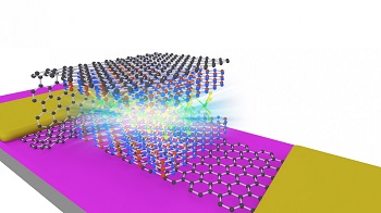
When atomically thin semiconductors are combined together in a Lego style, they emit light at a lower voltage potentially leading to low energy consumption devices.
Whilst this research is in its fundamental state this shows promise for practical applications in optoelectronics and telecommunications.
The voltage of an LED is usually equal to or larger than the bandgap energy per electron charge. A team of researchers based at The University of Manchester, University of Warsaw, the High Magnetic Field Laboratory in Grenoble and the National Institute for Materials Science in Japan have been able to demonstrate LEDs that turn on at much lower voltages.
The idea to stack layers of different materials to make so-called heterostructures goes back to the 1960s, when semiconductor gallium arsenide was researched for making miniature lasers—which are now widely used.
Today, heterostructures are common and are used very broadly in semiconductor industry as a tool to design and control electronic and optical properties in devices.
More recently in the era of atomically thin two-dimensional (2D) crystals, such as graphene, new types of heterostructures have emerged, where atomically thin layers are held together by relatively weak van der Waals forces.
The new structures nicknamed ‘van der Waals heterostructures’ open a huge potential to create numerous designer-materials and novel devices by stacking together any number of atomically thin layers. Hundreds of combinations become possible otherwise inaccessible in traditional three-dimensional materials, potentially giving access to new unexplored optoelectronic device functionality or unusual material properties.
There are a lot of experiments done by various research groups in the world, which focus on light emitting properties of transition metal dichalcogenides. However, often these studies are done purely by optical means. For practical applications, electrically triggered light emission is more desirable.
As published in Nature Communications, the team led by Dr Aleksey Kozikov, Professor Kostya Novoselov and Prof. Marek Potemski were able to do this using electricity. They bound electrons and holes sitting in different transition metal dichalcogenides, so-called interlayer excitons. The researchers created experimental conditions when these excitons recombine non-radiatively, Auger effect. The released energy is transferred to other carriers that can then move to higher energy states. As a result, charge carriers whose energy was originally too low to overcome the material’s bandgap can now easily cross this potential barrier, recombine and emit light. This effect is called upconversion.
Graphene electrodes are used to electrically inject charge carriers through hexagonal boron nitride stacked in a heterostructure into Molybdenum disulphide (MoS2) and Tungsten diselenide (WSe2). Changing the distance between these transition metal dichalcogenides by adding boron nitride in between allows tuning the LEDs from a normal operation to a low-voltage operation and observing the effect of upconversion.
From the fundamental point of view the observed effects mark an important step towards the realisation of exciton condensation and superfluidity of van der Waals heterostructures.
Dr. Johannes Binder, the first author of the paper, from the University of Warsaw said: “When we started measuring the first MoS2/WSe2 devices we were really surprised to observe emission at such low applied voltages. This upconverted emission impressively shows the importance of Auger processes for interlayer excitons in van der Waals heterostructures. Our findings shed more light on the physics in the largely unexplored high carrier density regime, which is crucial for optoelectronic applications as well as for fundamental phenomena like interlayer exciton condensation.”
Dr. Aleksey Kozikov added: “It is fascinating how adding just one atomically thin material can change properties of a device so dramatically. This is the power of van der Waals heterostructures in action”.
Share on:


Subscribe
Stay ahead of the technologies shaping the future of electronics with our latest newsletter, Advanced Electronics Packaging Digest. Get expert insights on advanced packaging, materials, and system-level innovation, delivered straight to your inbox.
Subscribe now to stay informed, competitive, and connected.
Suggested Items
AI Demand Drives PCB Material Market Growth
05/08/2026 | TPCAAs AI computing continues to drive a comprehensive upgrade in hardware specifications, the global printed circuit board industry is undergoing a profound structural transformation.
I-Connect007 Editor’s Choice: Five Must-Reads for the Week
05/01/2026 | Michelle Te, I-Connect007If it feels like the PCB industry is accelerating faster than ever, you’re not imagining it. From advanced materials driven by AI applications to renewed investment in domestic manufacturing—and the next generation stepping into critical roles—there’s a lot shifting at once. My selections for this week highlight where the pressure points are forming, and where the opportunities are emerging.
Electronics Manufacturing Needs Your Voice: Global Sentiment Survey Now Live
04/30/2026 | Global Electronics AssociationThe latest monthly Global Sentiment Survey from the Global Electronics Association is now open. At a time when demand uncertainty, policy shifts, energy costs, and supply chain recalibration are pulling the industry in multiple directions, the survey captures something macroeconomic data often misses: how manufacturers are actually experiencing conditions on the ground.
From Backbone to Breakthroughs: I-Connect007 Wraps PCB Materials Series with Focus on Innovation
05/06/2026 | I-Connect007I-Connect007 wraps up its six-part podcast series, PCB Materials: The Backbone and Future of Electronics, with Episode 6 and a discussion focusing on innovation. In Episode 6, Marcy LaRont speaks with Isola CTO Kirk Thompson about a critical turning point for the PCB industry as innovation accelerates. As data rates climb and demands from AI infrastructure, power density, flexible electronics, photonics, and chiplet integration intensify, traditional material assumptions are no longer sufficient.
Jiva Soluboard Getting the Attention It Deserves
04/30/2026 | Marcy LaRont, I-Connect007 MagazineJiva is a newer company that bridges the divide between PCB fabrication and product circularity or sustainability. Jiva Soluboard is the first fully recyclable laminate material ever created for PCB fabrication, and it's not going unnoticed. Stephen Driver, CEO of Jiva, gave us an update at APEX EXPO, including an exciting certification achievement in February.