


 Dan’s Biz Bookshelf: ‘Abundance: How We Build a Better Future’
 Trouble in Your Tank: In Complex Systems, Design Rules Aren’t Optional
 It’s Only Common Sense: The Phone Is Still Your Competitive Advantage


A Modified Device Fabrication Process Achieves Enhanced Spin Transport in Graphene
August 5, 2019 | ICN2Estimated reading time: 2 minutes
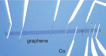
Researchers from the ICN2 Physics and Engineering of Nanodevices Group have proposed a modified graphene-based nanodevice fabrication technique that has increased up to three times the spin lifetime and relaxation length compared to previous work of the same kind. The work was fruit of the collaboration with Imec and K.U. Leuven (Belgium). The results have been published in 2D Materials and are expected to empower investigations on large-scale spintronic applications.
Spintronics is a field of research that was born in the 1980s. It amplifies the potential of traditional electronics by exploiting the electron’s spin degree of freedom, in addition to the usual state of charge. In the end, the goal is the same: to obtain devices to store, process and read information, but with enhanced characteristics such as lower power consumption, less heat dissipation, higher speed, etc. Although spintronics has not yet become as widespread as its conventional predecessor, some current devices are based on this new approach, such as magnetic hard disks, magnetic random access memories and magnetic sensors with varied applications in industrial environments, robotics and automotive industry.
Graphene is a promising material in this field. Spins can flow efficiently in it over long distances, meaning that they do not change their state (let’s say, from “up” to “down”) for a relatively long time. Due to its large-scale production, CVD graphene is becoming popular to fabricate spintronic devices. However, impurities arising from the graphene growth and device fabrication process limit its performance.
A team of scientists from the ICN2 Physics and Engineering of Nanodevices Group, led by ICREA Prof. Sergio O. Valenzuela, has proposed a high-yield device fabrication process from CVD graphene that has improved substantially its spin parameters. The work, whose first author is Zewdu M. Gebeyehu, was fruit of a collaboration with Imec and K.U. Leuven (Belgium). The results have been published in 2D Materials.
They demonstrate a spin signal measured across a 30 µm long channel with room-temperature spin lifetimes of up to 3 ns and spin relaxation lengths of up to 9 µm in monolayer graphene on SiO2/Si substrates. These spin parameters are the highest values for any form of graphene (both exfoliated and CVD graphene) on a standard SiO2/Si substrate.
To achieve this enhanced spin performance, the researchers used CVD graphene grown on a platinum foil and they modified the device fabrication technique so as to reduce the impurity levels associated with the graphene growth and fabrication steps. The latter requires the optimization of several standard processes, involving the preselection of high-quality uniform graphene with low level of impurities, an etching step combining e-beam lithography and oxygen plasma and a suitable post-annealing in high vacuum. The approach can be scaled and allows a highly reproducible fabrication of devices, which is the main requirement for potential industrialization.
The improvement on the spin parameters together with the reproducibility of the device fabrication process brings us closer to the realization of complex circuit architectures for spintronic devices such as spin logic and logic-in-memory for beyond CMOS computing.
Share on:


Subscribe
Stay ahead of the technologies shaping the future of electronics with our latest newsletter, Advanced Electronics Packaging Digest. Get expert insights on advanced packaging, materials, and system-level innovation, delivered straight to your inbox.
Subscribe now to stay informed, competitive, and connected.
Suggested Items
TLT Electronics Officially Opens Facility in Vietnam
05/06/2026 | TLT ElectronicsLithuanian EMS provider TLT Electronics has recently announced the opening of a new facility in Vietnam. For their clients, this is a chance to expand manufacturing into a second region without the headache of onboarding a new supplier. Same team, same processes, same quality standards — still TLT Manufacturing, just on another continent.
Trouble in Your Tank: In Complex Systems, Design Rules Aren’t Optional
05/06/2026 | Michael Carano -- Column: Trouble in Your TankThere is no question that the electronics industry, especially in circuit board design and fabrication, advanced packaging, and innovation throughout the value chain, has seen a significant transformation, whether it be in materials, system architecture, HDI and ultra HDI, semiconductors, or chiplets. AI and high-performance computing (HPC) are driving change across several fronts, including material properties, assembly techniques (think hybrid bonding), and power management.
Meet Emerging Engineers: Patrick Owen and Eric Mickenbecker, Summit Interconnect
05/05/2026 | Michelle Te, I-Connect007Patrick Owen and Eric Mickenbecker both work for Summit Interconnect, and are in their second year of the Global Electronics Association’s Emerging Engineer Program with mentor Brian Chislea. They stopped by the I-Connect007 booth at APEX EXPO and shared a bit of their story with me. Patrick has worked at the Hollister, California, plant since 2018, while Eric has been at the Chicago site since 2023. Like many of their peers, they came to the electronics industry from different paths, but are both excited about making an impact.
The Missing Connection: Wire Harness Quoting Joins the Digital Age
05/01/2026 | Joanne Harris, Tech-2marketingWalk the floor of a modern wire harness manufacturing facility, and the investment in technology is hard to miss. Automated wire cutting and stripping machines process thousands of cuts an hour with sub-millimeter precision. Computerized crimping presses deliver consistent, validated terminations that a hand tool never could. Laser wire markers, automated test benches, and vision-guided assembly stations represent hundreds of thousands of dollars of capital investment, all in service of building a better harness faster and more reliably than the competition.
EDADOC: Building the ‘Neural Hub’ for High-Compute Chips Within a Compact Space
04/28/2026 | ECIOEvery chip to the market must pass a stringent checkpoint before shipment known as ATE testing. Serving as the physical “neural hub” that connects test equipment worth millions of dollars with the device under test, the performance of the ATE test board directly determines the accuracy, efficiency, and final yield of chip testing. Amid the rapid rise of high-compute chips, what extreme challenges is this seemingly small circuit board facing? How is EDADOC addressing industry pain points through its one-stop “design + manufacturing” model?