


 Dan’s Biz Bookshelf: ‘Abundance: How We Build a Better Future’
 Trouble in Your Tank: In Complex Systems, Design Rules Aren’t Optional
 It’s Only Common Sense: The Phone Is Still Your Competitive Advantage


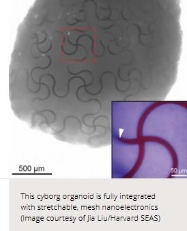
Cyborg Organoids Offer Rare View Into Early Stages of Development
August 12, 2019 | Harvard School of Engineering and Applied SciencesEstimated reading time: 2 minutes
What happens in the early days of organ development? How do a small group of cells organize to become a heart, a brain, or a kidney? This critical period of development has long remained the black box of developmental biology, in part because no sensor was small or flexible enough to observe this process without damaging the cells.
Now, researchers from the Harvard John A. Paulson School of Engineering and Applied Sciences (SEAS) have grown simplified organs known as organoids with fully integrated sensors. These so-called cyborg organoids offer a rare glimpse into the early stages of organ development.
“I was so inspired by the natural organ development process in high school, in which 3D organs start from few cells in 2D structures. I think if we can develop nanoelectronics that are so flexible, stretchable, and soft that they can grow together with developing tissue through their natural development process, the embedded sensors can measure the entire activity of this developmental process,” said Jia Liu, Assistant Professor of Bioengineering at SEAS and senior author of the study. “The end result is a piece of tissue with a nanoscale device completely distributed and integrated across the entire three-dimensional volume of the tissue.”
This type of device emerges from the work that Liu began as a graduate student in the lab of Charles M. Lieber, the Joshua and Beth Friedman University Professor. In Lieber’s lab, Liu once developed flexible, mesh-like nanoelectronics that could be injected in specific regions of tissue.
Building on that design, Liu and his team increased the stretchability of the nanoelectronics by changing the shape of the mesh from straight lines to serpentine structures (similar structures are used in wearable electronics). Then, the team transferred the mesh nanoelectronics onto a 2D sheet of stem cells, where the cells covered and interwove with the nanoelectronics via cell-cell attraction forces. As the stem cells began to morph into a 3D structure, the nanoelectronics seamlessly reconfigured themselves along with the cells, resulting in fully-grown 3D organoids with embedded sensors.
The stem cells were then differentiated into cardiomyocytes — heart cells — and the researchers were able to monitor and record the electrophysiological activity for 90 days.
“This method allows us to continuously monitor the developmental process and understand how the dynamics of individual cells start to interact and synchronize during the entire developmental process,” said Liu. “It could be used to turn any organoid into cyborg organoids, including brain and pancreas organoids.”
In addition to helping answer fundamental questions about biology, cyborg organoids could be used to test and monitor patient-specific drug treatments and potentially used for transplantations.
Share on:


Subscribe
Stay ahead of the technologies shaping the future of electronics with our latest newsletter, Advanced Electronics Packaging Digest. Get expert insights on advanced packaging, materials, and system-level innovation, delivered straight to your inbox.
Subscribe now to stay informed, competitive, and connected.
Suggested Items
TLT Electronics Officially Opens Facility in Vietnam
05/06/2026 | TLT ElectronicsLithuanian EMS provider TLT Electronics has recently announced the opening of a new facility in Vietnam. For their clients, this is a chance to expand manufacturing into a second region without the headache of onboarding a new supplier. Same team, same processes, same quality standards — still TLT Manufacturing, just on another continent.
Trouble in Your Tank: In Complex Systems, Design Rules Aren’t Optional
05/06/2026 | Michael Carano -- Column: Trouble in Your TankThere is no question that the electronics industry, especially in circuit board design and fabrication, advanced packaging, and innovation throughout the value chain, has seen a significant transformation, whether it be in materials, system architecture, HDI and ultra HDI, semiconductors, or chiplets. AI and high-performance computing (HPC) are driving change across several fronts, including material properties, assembly techniques (think hybrid bonding), and power management.
Meet Emerging Engineers: Patrick Owen and Eric Mickenbecker, Summit Interconnect
05/05/2026 | Michelle Te, I-Connect007Patrick Owen and Eric Mickenbecker both work for Summit Interconnect, and are in their second year of the Global Electronics Association’s Emerging Engineer Program with mentor Brian Chislea. They stopped by the I-Connect007 booth at APEX EXPO and shared a bit of their story with me. Patrick has worked at the Hollister, California, plant since 2018, while Eric has been at the Chicago site since 2023. Like many of their peers, they came to the electronics industry from different paths, but are both excited about making an impact.
The Missing Connection: Wire Harness Quoting Joins the Digital Age
05/01/2026 | Joanne Harris, Tech-2marketingWalk the floor of a modern wire harness manufacturing facility, and the investment in technology is hard to miss. Automated wire cutting and stripping machines process thousands of cuts an hour with sub-millimeter precision. Computerized crimping presses deliver consistent, validated terminations that a hand tool never could. Laser wire markers, automated test benches, and vision-guided assembly stations represent hundreds of thousands of dollars of capital investment, all in service of building a better harness faster and more reliably than the competition.
EDADOC: Building the ‘Neural Hub’ for High-Compute Chips Within a Compact Space
04/28/2026 | ECIOEvery chip to the market must pass a stringent checkpoint before shipment known as ATE testing. Serving as the physical “neural hub” that connects test equipment worth millions of dollars with the device under test, the performance of the ATE test board directly determines the accuracy, efficiency, and final yield of chip testing. Amid the rapid rise of high-compute chips, what extreme challenges is this seemingly small circuit board facing? How is EDADOC addressing industry pain points through its one-stop “design + manufacturing” model?