


 Flexible Thinking: Designing Flex Circuits for Dynamic Reliability
 Global PCB Connections: Rigid-flex and Flexible PCBs—The Backbone of Modern Electronics
 Happy’s Tech Talk #29: Bend-to-Install Semi-flex FR-4


What happens in the early days of organ development? How do a small group of cells organize to become a heart, a brain, or a kidney? This critical period of development has long remained the black box of developmental biology, in part because no sensor was small or flexible enough to observe this process without damaging the cells.
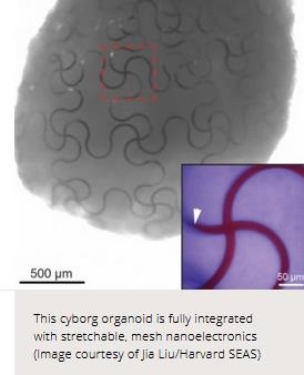
Now, researchers from the Harvard John A. Paulson School of Engineering and Applied Sciences (SEAS) have grown simplified organs known as organoids with fully integrated sensors. These so-called cyborg organoids offer a rare glimpse into the early stages of organ development.
“I was so inspired by the natural organ development process in high school, in which 3D organs start from few cells in 2D structures. I think if we can develop nanoelectronics that are so flexible, stretchable, and soft that they can grow together with developing tissue through their natural development process, the embedded sensors can measure the entire activity of this developmental process,” said Jia Liu, Assistant Professor of Bioengineering at SEAS and senior author of the study. “The end result is a piece of tissue with a nanoscale device completely distributed and integrated across the entire three-dimensional volume of the tissue.”
This type of device emerges from the work that Liu began as a graduate student in the lab of Charles M. Lieber, the Joshua and Beth Friedman University Professor. In Lieber’s lab, Liu once developed flexible, mesh-like nanoelectronics that could be injected in specific regions of tissue.
Building on that design, Liu and his team increased the stretchability of the nanoelectronics by changing the shape of the mesh from straight lines to serpentine structures (similar structures are used in wearable electronics). Then, the team transferred the mesh nanoelectronics onto a 2D sheet of stem cells, where the cells covered and interwove with the nanoelectronics via cell-cell attraction forces. As the stem cells began to morph into a 3D structure, the nanoelectronics seamlessly reconfigured themselves along with the cells, resulting in fully-grown 3D organoids with embedded sensors.
The stem cells were then differentiated into cardiomyocytes — heart cells — and the researchers were able to monitor and record the electrophysiological activity for 90 days.
“This method allows us to continuously monitor the developmental process and understand how the dynamics of individual cells start to interact and synchronize during the entire developmental process,” said Liu. “It could be used to turn any organoid into cyborg organoids, including brain and pancreas organoids.”
In addition to helping answer fundamental questions about biology, cyborg organoids could be used to test and monitor patient-specific drug treatments and potentially used for transplantations.


