


 Dan’s Biz Bookshelf: ‘Abundance: How We Build a Better Future’
 Trouble in Your Tank: In Complex Systems, Design Rules Aren’t Optional
 It’s Only Common Sense: The Phone Is Still Your Competitive Advantage


Development of Simplified New Mass Spectrometric Technique using Laser and Graphene
August 13, 2019 | DGISTEstimated reading time: 2 minutes
A technology that can obtain high-resolution, micrometer-sized images for mass spectrometric analysis without sample preparation has been developed. DGIST Research Fellow Jae Young Kim and Chair-professor Dae Won Moon’s team succeeded in developing the precise analysis and micrometer-sized imaging of bio samples using a small and inexpensive laser.
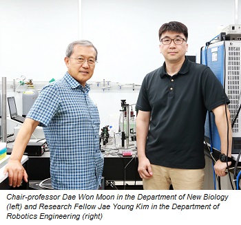
DGIST announced that Research Fellow Jae Young Kim in the Department of Robotics Engineering and Chair-professor Dae Won Moon’s team developed a technology that can analyze experiment samples without any preparation processing. Due to its ability to obtain high-resolution mass spectrometric images without an experimental environment using ‘continuous wave laser, the technology is expected to be applied widely in the precise medicine and medical diagnosis fields.
Many advance preparations are needed for the mass spectrometric imaging of biometric samples using ‘specimen,’ which thinly cut an object to analyze. The specimen must be changed artificially since they cannot be analyzed accurately in a room temperature or atmospheric pressure. To develop a convenient analysis technology and ease the burden, Research Fellow Kim started the research.
The research team installed a lens carrying continuous wave laser right below a microscope substrate where the specimen is put and shot the laser on it to measure mass spectra by examining molecules from desorption.
The mass spectra can be analyzed through a continuous wave laser whose energy is weaker than other lasers because of the use of ‘graphene substrate’ below the specimen.
Since the honeycomb-patterned graphene has very high heat conductivity and can convert light into heat, it can secure enough heat needed for specimen analysis with small amount of light generated by the continuous wave laser. This technology is also advantageous for obtaining high-resolution analysis images, because it can secure space to observe specimen much more closely even when using a 20x magnifying lens.
Chair-professor Dae Won Moon in the Department of New Biology explained that “Through this technology, we could greatly shorten the preparation time for analysis by omitting the specimen preprocessing step. Our next plan is to develop the technology further so it can be applied in various areas such as medical diagnosis.”
This research was participated by Research Fellow Jae Young Kim in the Department of Robotics Engineering and Ph.D. candidate Heejin Lim in the Department of New Biology as the co-first authors and was conducted with Professor Cheol Song in the Department of Robotics Engineering at DGIST, Professor Dong-Kwon Lim at Korea University, and Research Professor Ji-Won Park at Chungnam National University.
Share on:


Subscribe
Stay ahead of the technologies shaping the future of electronics with our latest newsletter, Advanced Electronics Packaging Digest. Get expert insights on advanced packaging, materials, and system-level innovation, delivered straight to your inbox.
Subscribe now to stay informed, competitive, and connected.
Suggested Items
Sony Semiconductor Solutions, TSMC Enter Preliminary Agreement for Next-Generation Image Sensor Strategic Partnership
05/08/2026 | TSMCSony Semiconductor Solutions Corporation and TSMC announced the signing of a non-binding memorandum of understanding (MOU) to form a strategic partnership for the development and manufacturing of next-generation image sensors.
BGA Technology Expands Inspection Capabilities with Creative Electron TruView X-ray System
05/08/2026 | BGA TechnologyBGA Technology, a leading provider of advanced electronics testing and inspection services, has enhanced its inspection capabilities with the addition of a Creative Electron TruView™ Simplex X-ray system at its Holbrook, New York facility.
Molex Completes Acquisition of Teramount Ltd.
05/07/2026 | PRNewswireMolex, a global electronics leader and connectivity innovator, has completed the acquisition of Teramount Ltd., an Israel‑based developer of detachable fiber‑to‑chip connectivity solutions optimized for high‑volume Co‑Packaged Optics (CPO) and other silicon photonics applications.
IBM, Aramco Explore Collaboration to Accelerate AI and Innovation Across Saudi Arabia
05/07/2026 | IBMAramco and IBM announced their intended collaboration on opportunities to advance artificial intelligence, agentic AI, automation, material science and other mutually agreed domains in the industrial sector.
Foxconn Launches Second-Gen LEO Satellite, Begins Inter-Satellite Link Testing
05/05/2026 | FoxconnFoxconn Technology Group, the world's largest electronics manufacturing services provider, announced that its second-generation low-Earth orbit (LEO) satellites, "Pearl-1A" and "Pearl-1B," were successfully launched into their designated orbits via SpaceX's Falcon 9 rocket on the evening of May 3 (Taipei time).