


 Flexible Thinking: Designing Flex Circuits for Dynamic Reliability
 Global PCB Connections: Rigid-flex and Flexible PCBs—The Backbone of Modern Electronics
 Happy’s Tech Talk #29: Bend-to-Install Semi-flex FR-4


Introduction
Flexible hybrid electronics (FHE) refers to a category of flexible electronics that are made through a combination of traditional assembly process of electronic components with high-precision ink printing technologies . By integrating silicon components with printed inks and flexible substrates, FHE will revolutionize the IoT and wearable industries. With FHE, designers can create a heterogeneous electronic system that can be fully integrated with different sensors, lighter in weight, more cost effective, more flexible and conforming to the curves of a human body or even stretchable across the shape of an object or structure—all while preserving the full functionality of traditional electronic systems.
The FHE industry is still in the early stages of development, and a variety of design, material, assembly and reliability issues need to be addressed. For example, electrical interconnections formed with conductive adhesives may not be as conductive or reliable as compared to conventional solder assembly. Typical polymer-based conductive inks are not as conductive as the etched copper used to make circuit boards and they are mostly not readily solderable. Additionally, commercially available stretchable thermoplastic-based film substrates have relatively low heat resistance and cannot withstand the current lead-free reflow process temperatures.
This article will present a hybrid manufacturing process to manufacture FHE systems with a two-layer interconnect structure utilizing screen printing of silver conductive ink, filled microvias to connect ink traces at the different layers, and use of the traditional reflow process to attach the semiconductor chips to the printed substrates.
Experimental
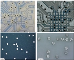
This study is to convert a rigid multilayer wearable development platform into a flexible one using printed conductive ink and flexible substrate. The current rigid platform contains two active semiconductor components and dozens of passive devices. The largest component is the microprocessor chip. Figure 1 shows the footprint for the microprocessor chip. It is an LGA package with 8X8 array and 64 I/Os. The pad size is 250 mm and the pitch is 400 mm, which leaves the space between pads at 150 mm.
To read this entire article, which appeared in the July 2019 issue of Design007 Magazine, click here.


