


 Dan’s Biz Bookshelf: ‘Abundance: How We Build a Better Future’
 Trouble in Your Tank: In Complex Systems, Design Rules Aren’t Optional
 It’s Only Common Sense: The Phone Is Still Your Competitive Advantage


A Laser for Penetrating Waves
August 16, 2019 | HZDREstimated reading time: 4 minutes
The "Landau-level laser" is an exciting concept for an unusual radiation source. It has the potential to efficiently generate so-called terahertz waves, which can be used to penetrate materials as well as for future data transmission. So far, however, nearly all attempts to make such a laser reality have failed. An international team of researchers has now taken an important step in the right direction: In the journal Nature Photonics (DOI: 10.1038/s41566-019-0496-1), they describe a material that generates terahertz waves by simply applying an electric current. Physicists from the German research center Helmholtz-Zentrum Dresden-Rossendorf (HZDR) played a significant role in this project.
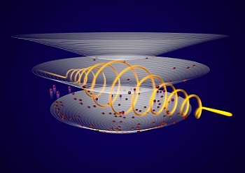
Image Caption: An international research team has been able to show that it is relatively easy to generate terahertz waves with an alloy of mercury, cadmium and tellurium. To examine the behavior of the electrons in the material, the physicists use the free-electron laser FELBE at HZDR. Circularly polarized terahertz pulses (orange spiral) excite the electrons (red) from the lowest to the next higher energy level (parabolic shell). The energy gap of these so-called Landau levels can be adjusted with the help of a magnetic field. Foto: HZDR / Juniks
Like light, terahertz waves are electromagnetic radiation, in a frequency range between microwaves and infrared radiation. Their properties are of great technological and scientific interest, as they allow fundamental researchers to study the oscillations of crystal lattices or the propagation of spin waves. Simultaneously “terahertz waves are of interest for technical applications because they can penetrate numerous substances that are otherwise opaque, such as clothing, plastics and paper,” Stephan Winnerl from HZDR's Institute of Ion Beam Physics and Materials Research explains. Terahertz scanners are already used today for airport security checks, detecting whether passengers are concealing dangerous objects under their clothing – without having to resort to harmful X-rays.
Because terahertz waves have a higher frequency than the radio waves we use today, they could also be harnessed for data transmission one day. Current WLAN technology, for instance, operates at frequencies of two to five gigahertz. Since terahertz frequencies are about a thousand times higher, they could transmit images, video, and music much faster, albeit across shorter distances. However, the technology is not yet fully developed. “There has been a lot of progress in recent years,” Winnerl reports. “But generating the waves is still a challenge - experts speak of a veritable terahertz gap.” A particular issue is the lack of a terahertz laser that is compact, powerful, and tunable at the same time.
Flexible Frequencies
Laser light is generated by the electrons in the laser material. According to the quantum effect, energized electrons emit light, but they cannot absorb just any random amount of energy, only certain portions. Accordingly, light is also emitted in portions, in a specific color and as a focused beam. For some time now, experts have set their sights on a specific concept for a terahertz laser: the “Landau-level laser”. It is special because it can use a magnetic field to flexibly adjust the electrons’ energy levels. These levels, in turn, determine the frequencies that are emitted by the electrons, which makes the laser tunable – a huge advantage for many scientific and technical applications.
There is just one issue: Such a laser does not exist yet. “So far, the problem has been that the electrons pass their energy on to other electrons instead of emitting them as the desired light waves,” Winnerl explains. Experts call this physical process the “Auger effect”. To their chagrin, this phenomenon also occurs in graphene, a material that they deemed particularly promising for a “Landau-level laser”. This two-dimensional form of carbon showed strong Auger scattering in HZDR experiments.
A Question of Material
The research team therefore tried another material: a heavy metal alloy of mercury, cadmium, and tellurium (HgCdTe) that is used for highly sensitive thermal imaging cameras, among other things. The special feature of this material is that its mercury, cadmium, and tellurium contents can be very precisely chosen, which makes it possible to fine-tune a certain property that experts call the “band gap”.
As a result, the material showed properties similar to graphene, but without the issue of strong Auger scattering. “There are subtle differences to graphene that avoid this scattering effect,” says Stephan Winnerl. “Put simply, the electrons can’t find any other electrons that could absorb the right amount of energy.” Therefore, they have no choice but to get rid of their energy in the form that the scientists want: terahertz radiation.
The project was an international team effort: Russian partners had prepared the HgCdTe samples, which the project’s lead group in Grenoble then analyzed. One of the pivotal investigations took place in Dresden-Rossendorf: Using the free-electron laser FELBE, experts fired strong terahertz pulses at the sample and were able to observe the electrons’ behavior in temporal resolution. The result: “We noticed that the Auger effect that we had observed in graphene had actually disappeared,” Winnerl is happy to report.
LED for Terahertz
Lastly, a work group in Montpellier observed that the HgCdTe compound actually emits terahertz waves when electric current is applied. By varying an additional magnetic field of only about 200 millitesla, the experts were able to vary the frequency of the emitted waves in a range of one to two terahertz – a tunable radiation source. “It’s not quite a laser yet, but rather like a terahertz LED,” Winnerl describes. “But we should be able to extend the concept to a laser, even though it will take some effort.” And that’s exactly what the French partners want to tackle next.
There is one limiting factor, however: Up to now, the principle has only worked when cooled to very low temperatures, just above absolute zero. “This is certainly a hindrance for everyday applications,” Winnerl summarizes. “But for use in research and in certain high-tech systems, we should be able to make it work with this kind of cooling.”
Share on:


Subscribe
Stay ahead of the technologies shaping the future of electronics with our latest newsletter, Advanced Electronics Packaging Digest. Get expert insights on advanced packaging, materials, and system-level innovation, delivered straight to your inbox.
Subscribe now to stay informed, competitive, and connected.
Suggested Items
Gregoire Outters Promoted to President of Teledyne Marine Group
04/06/2026 | TeledyneTeledyne Technologies Incorporated announced the promotion of Gregoire Outters to President of its Teledyne Marine Group.
Teledyne Strengthens Commitment to the Space Sector
04/01/2026 | BUSINESS WIRETeledyne Technologies Incorporated is excited to announce the integration of the company’s extensive portfolio of space-focused technologies and businesses, reinforcing its long-term commitment to the global space sector.
Teledyne to Supply Detectors for Lazuli Space Observatory
03/30/2026 | BUSINESS WIRETeledyne Space Imaging, part of Teledyne Technologies Incorporated has been awarded a contract by Schmidt Sciences to deliver advanced near-infrared (NIR) H4RG-10 flight focal plane arrays (FPAs) and custom electronics for integration into the Integral Field Spectrograph on the groundbreaking Lazuli Space Observatory.
New Superconducting Chip Could Enable Breakthrough Nondestructive Terahertz Imaging
03/23/2026 | University of GlasgowA tiny crystal chip which uses terahertz radiation to see clearly through a wide range of materials could find applications in healthcare, biological research, and security screening.
The Test Connection Adds Creative Electron Prime TruVision™ X-ray and CT System for Deeper Failure Analysis
03/05/2026 | TTCIThe Test Connection Inc. (TTCI), a trusted provider of electronic test and manufacturing solutions for more than 45 years, has added the Prime TruVision™ X-ray and computed tomography (CT) inspection system from Creative Electron to its engineering and analysis services.