


 The Marketing Minute: Marketing With Layers
 The Right Approach: Electro-Tek—A Williams Family Legacy, Part 1
 It’s Only Common Sense: If You’re Not Differentiated, You’re Dead


Graphene Goes Mainstream
August 19, 2019 | UC Santa BarbaraEstimated reading time: 5 minutes
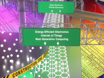
Ever since graphene, the flexible, two-dimensional form of graphite (think a 1-atom-thick sheet of pencil lead), was discovered in 2004, researchers around the world have been working to develop commercially scalable applications for this high-performance material.
Graphene is 100 to 300 times stronger than steel and has a maximum electrical current density orders of magnitude greater than that of copper, making it the strongest, thinnest and, by far, the most reliable electrically conductive material on the planet. It is, therefore, an extremely promising material for interconnects, the fundamental components that connect billions of transistors on microchips in computers and other electronic devices in the modern world.
For over two decades, interconnects have been made of copper, but that metal encounters fundamental physical limitations as electrical components that incorporate it shrink to the nanoscale. “As you reduce the dimensions of copper wires, their resistivity shoots up,” said Kaustav Banerjee, a professor in the Department of Electrical and Computer Engineering. “Resistivity is a material property that is not supposed to change, but at the nanoscale, all properties change.”
As the resistivity increases, copper wires generate more heat, reducing their current-carrying capacity. It’s a problem that poses a fundamental threat to the $500 billion semiconductor industry. Graphene has the potential to solve that and other issues. One major obstacle, though, is designing graphene micro-components that can be manufactured on-chip, on a large scale, in a commercial foundry.
“Whatever the component, be it inductors, interconnects, antennas or anything else you want to do with graphene, industry will move forward with it only if you find a way to synthesize graphene directly onto silicon wafers,” Banerjee said. He explained that all manufacturing processes related to the transistors, which are made first, are referred to as the ‘front end.’ To synthesize something at the back-end — that is, after the transistors are fabricated — you face a tight thermal budget that cannot exceed a temperature of about 500 degrees Celsius. If the silicon wafer gets too hot during the back-end processes employed to fabricate the interconnects, other elements that are already on the chip may get damaged, or some impurities may start diffusing, changing the characteristics of the transistors.
Now, after a decade-long quest to achieve graphene interconnects, Banerjee’s lab has developed a method to implement high-conductivity, nanometer-scale doped multilayer graphene (DMG) interconnects that are compatible with high-volume manufacturing of integrated circuits. A paper describing the novel process was named one of the top papers at the 2018 IEEE International Electron Devices Meeting (IEDM), from more than 230 that were accepted for oral presentations. It also was one of only two papers included in the first annual “IEDM Highlights” section of an issue of the journal Nature Electronics.
Banerjee first proposed the idea of using doped multi-layer graphene at the 2008 IEDM conference and has been working on it ever since. In February 2017 he led the experimental realization of the idea by Chemical Vapor Deposition (CVD) of multilayer graphene at a high temperature, subsequently transferring it to a silicon chip, then patterning the multilayer graphene, followed by doping. Electrical characterization of the conductivity of DMG interconnects down to a width of 20 nanometers established the efficacy of the idea that was proposed in 2008. However, the process was not “CMOS-compatible” (the standard industrial-scale process for making integrated circuits), since the temperature of CVD processes far exceed the thermal budget of back-end processes.
To overcome this bottleneck, Banerjee’s team developed a unique pressure-assisted solid-phase diffusion method for directly synthesizing a large area of high-quality multilayer graphene on a typical dielectric substrate used in the back-end CMOS process. Solid-phase diffusion, well known in the field of metallurgy and often used to form alloys, involves applying pressure and temperature to two different materials that are in close contact so that they diffuse into each other.
Banerjee’s group employed the technique in a novel way. They began by depositing solid-phase carbon in the form of graphite powder onto a deposited layer of nickel metal of optimized thickness. Then they applied heat (300 degrees Celsius) and nominal pressure to the graphite powder to help break down the graphite. The high diffusivity of carbon in nickel allows it to pass rapidly through the metal film.
How much carbon flows through the nickel depends on its thickness and the number of grains it holds. “Grains” refer to the fact that deposited nickel is not a single-crystal metal, but rather a polycrystalline metal, meaning it has areas where two single-crystalline regions meet each other without being perfectly aligned. These areas are called grain boundaries, and external particles — in this case, the carbon atoms — easily diffuse through them. The carbon atoms then recombine on the other surface of the nickel closer to the dielectric substrate, forming multiple graphene layers.
Banerjee’s group is able to control the process conditions to produce graphene of optimal thickness. “For interconnect applications, we know how many layers of graphene are needed,” said Junkai Jiang, a Ph.D. candidate in Banerjee’s lab and lead author of the 2018 IEDM paper. “So we optimized the nickel thickness and other process parameters to obtain precisely the number of graphene layers we want at the dielectric surface. “Subsequently, we simply remove the nickel by etching so that what’s left is only very high-quality graphene — virtually the same quality as graphene grown by CVD at very high temperatures,” he continued. “Because our process involves relatively low temperatures that pose no threat to the other fabricated elements on the chip, including the transistors, we can make the interconnects right on top of them.”
UCSB has filed a provisional patent on the process, which overcomes the obstacles that, until now, have prevented graphene from replacing copper. Bottom line: graphene interconnects help to create faster, smaller, lighter, more flexible, more reliable and more cost-effective integrated circuits. Banerjee is currently in talks with industry partners interested in potentially licensing this CMOS-compatible graphene synthesis technology, which could pave the way for what would be the first 2D material to enter the mainstream semiconductor industry.
According to Intel’s Tahir Ghani, senior fellow of technology development, and director of the firm’s Pathfinding Group in Hillsboro, Oregon, “Doped multilayer graphene films appear to be a promising contender to replace copper interconnects, which are plagued by dramatic resistance increase at aggressively scaled wire dimensions. The innovation in low-temperature growth of high-quality graphene films by Professor Banerjee and his team at UCSB is a critical first step to enable successful integration of graphene interconnects into existing CMOS transistor technology. The remaining work involving graphene interconnects includes further investigation of its ultimate scalability and contact resistance.”
Support for the research has come from various sources over the years, including the National Science Foundation, the National Institute of Standards and Technology, Semiconductor Research Corporation, and currently, the U.S. Army Research Office and the University of California Research Initiatives.
Share on:


Testimonial
"In a year when every marketing dollar mattered, I chose to keep I-Connect007 in our 2025 plan. Their commitment to high-quality, insightful content aligns with Koh Young’s values and helps readers navigate a changing industry. "
Brent Fischthal - Koh YoungSuggested Items
Episode 6 of Ultra HDI Podcast Series Explores Copper-filled Microvias in Advanced PCB Design and Fabrication
10/15/2025 | I-Connect007I-Connect007 has released Episode 6 of its acclaimed On the Line with... American Standard Circuits: Ultra High Density Interconnect (UHDI) podcast series. In this episode, “Copper Filling of Vias,” host Nolan Johnson once again welcomes John Johnson, Director of Quality and Advanced Technology at American Standard Circuits, for a deep dive into the pros and cons of copper plating microvias—from both the fabricator’s and designer’s perspectives.
Nolan’s Notes: Tariffs, Technologies, and Optimization
10/01/2025 | Nolan Johnson -- Column: Nolan's NotesLast month, SMT007 Magazine spotlighted India, and boy, did we pick a good time to do so. Tariff and trade news involving India was breaking like a storm surge. The U.S. tariffs shifted India from one of the most favorable trade agreements to the least favorable. Electronics continue to be exempt for the time being, but lest you think that we’re free and clear because we manufacture electronics, steel and aluminum are specifically called out at the 50% tariff levels.
MacDermid Alpha & Graphic PLC Lead UK’s First Horizontal Electroless Copper Installation
09/30/2025 | MacDermid Alpha & Graphic PLCMacDermid Alpha Electronics Solutions, a leading supplier of integrated materials and chemistries to the electronics industry, is proud to support Graphic PLC, a Somacis company, with the installation of the first horizontal electroless copper metallization process in the UK.
Electrodeposited Copper Foils Market to Grow by $11.7 Billion Over 2025-2032
09/18/2025 | Globe NewswireThe global electrodeposited copper foils market is poised for dynamic growth, driven by the rising adoption in advanced electronics and renewable energy storage solutions.
MacDermid Alpha Showcases Advanced Interconnect Solutions at PCIM Asia 2025
09/18/2025 | MacDermid Alpha Electronics SolutionsMacDermid Alpha Electronic Solutions, a global leader in materials for power electronics and semiconductor assembly, will showcase its latest interconnect innovations in electronic interconnect materials at PCIM Asia 2025, held from September 24 to 26 at the Shanghai New International Expo Centre, Booth N5-E30