


 The Marketing Minute: Marketing With Layers
 The Right Approach: Electro-Tek—A Williams Family Legacy, Part 1
 It’s Only Common Sense: If You’re Not Differentiated, You’re Dead


Scientists Report Two Advances in Understanding the Role of ‘Charge Stripes’ in Superconducting Materials
August 21, 2019 | SLAC National Accelerator LaboratoryEstimated reading time: 3 minutes
High-temperature superconductors, which carry electricity with zero resistance at much higher temperatures than conventional superconducting materials, have generated a lot of excitement since their discovery more than 30 years ago because of their potential for revolutionizing technologies such as maglev trains and long-distance power lines. But scientists still don’t understand how they work.
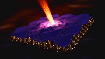
Image Caption: This cutaway view shows stripes of higher and lower electron density—“charge stripes”—within a copper-based superconducting material. Experiments with SLAC’s X-ray laser directly observed how those stripes fluctuate when hit with a pulse of light, a step toward understanding how they interact with high-temperature superconductivity. (Greg Stewart/SLAC National Accelerator Laboratory)
One piece of the puzzle is the fact that charge density waves – static stripes of higher and lower electron density running through a material—have been found in one of the major families of high-temperature superconductors, the copper-based cuprates. But do these charge stripes enhance superconductivity, suppress it or play some other role?
In independent studies, two research teams report important advances in understanding how charge stripes might interact with superconductivity. Both studies were carried out with X-rays at the Department of Energy’s SLAC National Accelerator Laboratory.
Exquisite Detail
In a paper published today in Science Advances, researchers from the University of Illinois at Urbana-Champaign (UIUC) used SLAC’s Linac Coherent Light Source (LCLS) X-ray free-electron laser to observe fluctuations in charge density waves in a cuprate superconductor.
They disturbed the charge density waves with pulses from a conventional laser and then used RIXS, or resonant inelastic X-ray scattering, to watch the waves recover over a period of a few trillionths of a second. This recovery process behaved according to a universal dynamical scaling law: It was the same at all scales, much as a fractal pattern looks the same whether you zoom in or zoom out.
With LCLS, the scientists were able to measure, for the first time and in exquisite detail, exactly how far and how fast the charge density waves fluctuated. To their surprise, the team discovered that the fluctuations were not like the ringing of a bell or the bouncing of a trampoline; instead, they were more like the slow diffusion of a syrup—a quantum analog of liquid crystal behavior, which had never been seen before in a solid.
“Our experiments at LCLS establish a new way to study fluctuations in charge density waves, which could lead to a new understanding of how high-temperature superconductors operate,” says Matteo Mitrano, a postdoctoral researcher in professor Peter Abbamonte’s group at UIUC.
This team also included researchers from Stanford University, the National Institute of Standards and Technology and Brookhaven National Laboratory.
Hidden Arrangements
Another study, reported last month in Nature Communications, used X-rays from SLAC’S Stanford Synchrotron Radiation Lightsource (SSRL) to discover two types of charge density wave arrangements, making a new link between these waves and high-temperature superconductivity.
Led by SLAC scientist Jun-Sik Lee, the research team used RSXS, or resonant soft X-ray scattering, to watch how temperature affected the charge density waves in a cuprate superconductor.
“This resolves a mismatch in data from previous experiments and charts a new course for fully mapping the behaviors of electrons in these exotic superconducting materials,” Lee says.
“I believe that exploring new or hidden arrangements, as well as their intertwining phenomena, will contribute to our understanding of high-temperature superconductivity in cuprates, which will inform researchers in their quest to design and develop new superconductors that work at warmer temperatures.”
The team also included researchers from Stanford, Pohang Accelerator Laboratory in South Korea and Tohoku University in Japan.
SSRL and LCLS are DOE Office of Science user facilities. Both studies were supported by the Office of Science.
Share on:


Testimonial
"In a year when every marketing dollar mattered, I chose to keep I-Connect007 in our 2025 plan. Their commitment to high-quality, insightful content aligns with Koh Young’s values and helps readers navigate a changing industry. "
Brent Fischthal - Koh YoungSuggested Items
Episode 6 of Ultra HDI Podcast Series Explores Copper-filled Microvias in Advanced PCB Design and Fabrication
10/15/2025 | I-Connect007I-Connect007 has released Episode 6 of its acclaimed On the Line with... American Standard Circuits: Ultra High Density Interconnect (UHDI) podcast series. In this episode, “Copper Filling of Vias,” host Nolan Johnson once again welcomes John Johnson, Director of Quality and Advanced Technology at American Standard Circuits, for a deep dive into the pros and cons of copper plating microvias—from both the fabricator’s and designer’s perspectives.
Nolan’s Notes: Tariffs, Technologies, and Optimization
10/01/2025 | Nolan Johnson -- Column: Nolan's NotesLast month, SMT007 Magazine spotlighted India, and boy, did we pick a good time to do so. Tariff and trade news involving India was breaking like a storm surge. The U.S. tariffs shifted India from one of the most favorable trade agreements to the least favorable. Electronics continue to be exempt for the time being, but lest you think that we’re free and clear because we manufacture electronics, steel and aluminum are specifically called out at the 50% tariff levels.
MacDermid Alpha & Graphic PLC Lead UK’s First Horizontal Electroless Copper Installation
09/30/2025 | MacDermid Alpha & Graphic PLCMacDermid Alpha Electronics Solutions, a leading supplier of integrated materials and chemistries to the electronics industry, is proud to support Graphic PLC, a Somacis company, with the installation of the first horizontal electroless copper metallization process in the UK.
Electrodeposited Copper Foils Market to Grow by $11.7 Billion Over 2025-2032
09/18/2025 | Globe NewswireThe global electrodeposited copper foils market is poised for dynamic growth, driven by the rising adoption in advanced electronics and renewable energy storage solutions.
MacDermid Alpha Showcases Advanced Interconnect Solutions at PCIM Asia 2025
09/18/2025 | MacDermid Alpha Electronics SolutionsMacDermid Alpha Electronic Solutions, a global leader in materials for power electronics and semiconductor assembly, will showcase its latest interconnect innovations in electronic interconnect materials at PCIM Asia 2025, held from September 24 to 26 at the Shanghai New International Expo Centre, Booth N5-E30