


 The Right Approach: Get Ready for ISO 9001 Version 6
 Dan’s Biz Bookshelf: ‘Still Broke: Walmart’s Remarkable Transformation'
 Driving Innovation: Depth Routing Processes—Achieving Unparalleled Precision in Complex PCBs


Scientists Develop a Metamaterial for Applications in Magnonics, an Alternative to Conventional Electronics
August 23, 2019 | MIPTEstimated reading time: 3 minutes
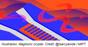
Physicists from Russia and Europe have demonstrated the real possibility of using superconductor/ferromagnet systems to create magnonic crystals, which will be at the core of spin-wave devices to come in the post-silicon era of electronics.
Magnonics investigates the possibilities of using spin waves to transmit and process information. Whereas photonics deals with photons and electromagnetic waves, the focus of magnonics is on spin waves, or magnons, which are harmonic oscillations of the orientation of magnetic moments. In ferromagnetic materials, the magnetic moments of the electrons, i.e., their spins, are aligned in a magnetic field. The waves of spin alignment observed in a magnetic system are called spin waves.
Magnonics is seen as a promising research area in post-silicon wave electronics, as spin waves have a number of advantages over, say, microwave photons. For instance, spin waves can be controlled by an external magnetic field. Microwaves, which are essentially electromagnetic waves, have an average wavelength of one centimeter, whereas spin waves in the same microwave frequency range have wavelengths of micrometers. This is why these controllable waves can be used to build very compact microdevices for microwave signals.
Magnonic crystals are the most fundamental systems (sometimes referred to as the building blocks) required to build a device that operates using spin wave signals. These crystals have a wide range of potential applications and will lie at the heart of frequency filters, grating couplers, waveguides, and magnonic devices, which are analogs of transistors.
The authors of this study tested their basic hypothesis, which was as follows: Can a magnonic crystal be created using a ferromagnet/superconductor hybrid system? Ferromagnetism and superconductivity are two antagonistic phenomena. In a superconductor, the spins of the electrons bound into a Cooper pair are oriented in opposite directions, whereas in ferromagnets, they tend to align in the same direction. Scientists have traditionally tried to influence superconducting properties with ferromagnetism.
“The last couple of years, we have been successful achieving the reverse. First, we examine ferromagnetic systems and see if their ferromagnetic properties can somehow be modified using superconductors. This is why it has attracted global interest,” explains Dr. Igor Golovchanskiy, a co-author of the study and researcher at MIPT’s Laboratory of Topological Quantum Phenomena in Superconducting Systems. “Initially, magnonics included only room-temperature investigations. Therefore, hybridization of ferromagnets with superconductors, which do not exist at room temperature, was out of the question. Besides, ferromagnetism has traditionally been considered “stronger” than superconductivity and, hence, can’t be influenced by it. Our laboratory studies cryogenic systems, and we set ourselves a goal to look at how magnonic systems behave at cryogenic temperatures when they are forced to interact with superconductors.”
The main result of this research is that the scientists have proved it possible to work with magnonic crystals using the superconductor/ferromagnet hybrid system. The scientists have also observed a peculiar magnonic band structure in their architecture characterized by the presence of forbidden bands in the gigahertz frequency range.
The research was conducted in three stages: a sample was fabricated and measured, and then simulations were performed. The system consisted of a regular superconducting niobium (Nb) structure placed on top of a ferromagnetic Ni80Fe20 permalloy (Py) thin film.
Figure 1. A schematic representation of spin waves traveling through the metamaterial and the resultant wave spectrum, reflecting the properties of an artificial crystal
The system was placed in a cryostat, and the microwave signal transmission coefficient was measured. If the value was the same as the fundamental frequencies of the system, resonance absorption was observed. This is called ferromagnetic resonance. The obtained spectrum showed two lines, indicating that the periodic structure consisted of two bound areas with alternating ferromagnetic resonance conditions. The ferromagnetic properties were modulated by means of the superconducting structure.
During the third stage, “micromagnetic simulations” were performed. This helped the researchers recreate the magnonic band structure, which is formed by allowed and forbidden bands with a different geometry.
The technological process of the development of silicon-based microelectronic components is reaching the theoretical limit of available sizes. As a result, a further increase in computational capacity, and hence the continued miniaturization of components, requires new approaches. In this regard, the investigated superconductor/ferromagnet systems offer good prospects for wave electronics, since the critical sizes for superconducting materials are less than a micrometer. Therefore, it is possible to make superconducting elements very small.
The authors of the study believe the results of their research will find use in microwave electronics and magnonics, including the field of quantum magnonics. However, the range of potential applications is still limited as the system cannot survive at room temperature.
Share on:


Testimonial
"We’re proud to call I-Connect007 a trusted partner. Their innovative approach and industry insight made our podcast collaboration a success by connecting us with the right audience and delivering real results."
Julia McCaffrey - NCAB GroupSuggested Items
EV Group Achieves Breakthrough in Hybrid Bonding Overlay Control for Chiplet Integration
09/12/2025 | EV GroupEV Group (EVG), a leading provider of innovative process solutions and expertise serving leading-edge and future semiconductor designs and chip integration schemes, today unveiled the EVG®40 D2W—the first dedicated die-to-wafer overlay metrology platform to deliver 100 percent die overlay measurement on 300-mm wafers at high precision and speeds needed for production environments. With up to 15X higher throughput than EVG’s industry benchmark EVG®40 NT2 system designed for hybrid wafer bonding metrology, the new EVG40 D2W enables chipmakers to verify die placement accuracy and take rapid corrective action, improving process control and yield in high-volume manufacturing (HVM).
AV Switchblade 600 Loitering Munition System Achieves Pivotal Milestone with First-Ever Air Launch from MQ-9A
09/12/2025 | BUSINESS WIREAeroVironment, Inc. (AV) a global leader in intelligent, multi-domain autonomous systems, announced its Switchblade 600 loitering munition system (LMS) has achieved a significant milestone with its first-ever air launch from an MQ-9A Reaper Unmanned Aircraft System (UAS).
United Electronics Corporation Unveils Revolutionary CIMS Galaxy 30 Automated Optical Inspection System
09/11/2025 | United Electronics CorporationUnited Electronics Corporation (UEC) today announced the launch of its new groundbreaking CIMS Galaxy 30 Automated Optical Inspection (AOI) machine, setting a new industry standard for precision electronics manufacturing quality control. The Galaxy 30, developed and manufactured by CIMS, represents a significant leap forward in inspection technology, delivering exceptional speed improvements and introducing cutting-edge artificial intelligence capabilities.
IPS, SEL Raise the Bar for ENIG Automation in North America
09/11/2025 | Mike Brask, IPSIPS has installed a state-of-the-art automated ENIG plating line at Schweitzer Engineering Laboratories’ PCB facility in Moscow, Idaho. The 81-foot, fully enclosed line sets a new standard for automation, safety, and efficiency in North American PCB manufacturing and represents one of the largest fully enclosed final finish lines in operation.
Smart Automation: Odd-form Assembly—Dedicated Insertion Equipment Matters
09/09/2025 | Josh Casper -- Column: Smart AutomationLarge, irregular, or mechanically unique parts, often referred to as odd-form components, have never truly disappeared from electronics manufacturing. While many in the industry have been pursuing miniaturization, faster placement speeds, and higher-density PCBs, certain market sectors are moving in the opposite direction.