


 Driving Innovation: Depth Routing Processes—Achieving Unparalleled Precision in Complex PCBs
 It's Only Common Sense: The Evolution of Prospecting
 Dan's Biz Bookshelf: 'Apple in China: The Capture of the World’s Greatest Company'


Vertical Conductive Structures, Part 3: Design Tool Techniques
August 23, 2019 | Ed Hickey and Mike Catrambone, Cadence Design Systems, and Joan Tourné, Nextgin TechnologyEstimated reading time: 3 minutes
Editor’s Note: This article is part three of a series on vertical conductive structures. Click here to read Part 1 and Part 2.
As design complexity and density increases, it sometimes requires the designer to leverage different via technologies to successfully route into larger pin count devices while maintaining the highest level of signal integrity. Using through-hole vias can take up a lot of valuable board space; moving to smaller blind vias reduces the via size but will require larger buried vias to complete the connections deeper in the board. Another costly alternative is using every layer interconnect (ELIC) technology with each layer pair having its own copper-filled, laser-drilled microvias. Stacking these microvias on top of each other between layer pairs can extend the connection between any two layers in the board. These via technologies may successfully route the design but could cause the layer count to rise, and if not done correctly, could lead to signal integrity issues.
New vertical conductive structure (VeCS) technology can reduce layer count and improve signal integrity without the need for sequential technologies. VeCS is different than traditional through-hole vias, microvias, and ELIC designs, which are more expensive and require a high number of laminations, drilling, and plating cycles to build up a reasonable number of layers. Using VeCS combines routing channels for better utilization of the channel, escaping out large pin count devices. The larger routing channels allow more routes to escape with a more reliable/solid plane reference without the swiss-cheese effect normally seen with other via technologies.
In Allegro 17.2, VeCS structures are nothing more than a mechanical symbol that can be free-placed or placed inside of a ball grid array (BGA) field to take advantage of this new routing escape technology. No major changes were required to support these new structures in Allegro PCB Designer except for a manufacturing output update to generate limited depth (blind) drill files for pins in support of VeCS-2 blind depth structures. 17.2 Padstack Editor supports by-layer keepouts as well as adjacent layer keepouts to ensure manufacturability when these structures are used in a layout. These structures are created as library objects, so they can be easily leveraged across many designs for commonly used device escapes. If a structure requires a change, it can be made in one place with all instances refreshed in the layout.
VeCS
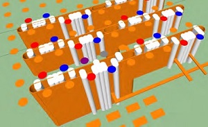
At the moment, we distinguish two “slot” technologies: VeCS-1, where the slots go through the board, and VeCS-2, where we do multi-level blind slots (Figure 1).
Figure 1: The front slot on the left side shows a VeCS-1, and the right shows VeCS-2.
In practice, we will see more hybrid constructions of VeCS-1 and VeCS-2 in one slot. The advantage is that we can connect GND and powers to multiple layers using VeCS-1, and the adjacent signal only connects to layer 4, for example. The VeCS-2 part of the slot creates a stubbles connection, minimizing capacitance and the dispersion of a higher speed signal.
At the moment, NextGIn Technology is very much focused on next-generation products, such as very high bandwidth applications where signal transitions between layers can be tuned such that the impedance of the vertical trace matches the impedance of the signal layer as it transits from one layer and connects to next. This enables layer transitions with minimum loss, enabling more efficient use of routing real estate compared to the ineffective and costly point-to-point routing used today using traditional via technology.
VeCS can be combined with through-hole, buried/blind vias, and microvia/HDI technology. There is no limitation. For example, a VeCS core/multilayer can be sandwiched between a set of microvias on top and bottom.
The process flow used right now is as follows:
1. Build board per standard flow.
2. Form slots (optional at mechanical drill stage): VeCS-1 and VeCS-2 from front and back.
3. Complete plating (standard).
4. Fill slots and holes (optional).
5. Form second route and bottom route.
6. Fill slots (second route).
7. Drill through-holes (optional).
8. Complete surface plating similar to a plated over-filled via (POFV).
9. Finish the panel as standard.
To read the full article, which appeared in the August 2019 issue of PCB007 Magazine, click here.
Share on:


Testimonial
"The I-Connect007 team is outstanding—kind, responsive, and a true marketing partner. Their design team created fresh, eye-catching ads, and their editorial support polished our content to let our brand shine. Thank you all! "
Sweeney Ng - CEE PCBSuggested Items
Closing the Loop on PCB Etching Waste
09/09/2025 | Shawn Stone, IECAs the PCB industry continues its push toward greener, more cost-efficient operations, Sigma Engineering’s Mecer System offers a comprehensive solution to two of the industry’s most persistent pain points: etchant consumption and rinse water waste. Designed as a modular, fully automated platform, the Mecer System regenerates spent copper etchants—both alkaline and acidic—and simultaneously recycles rinse water, transforming a traditionally linear chemical process into a closed-loop system.
Driving Innovation: Depth Routing Processes—Achieving Unparalleled Precision in Complex PCBs
09/08/2025 | Kurt Palmer -- Column: Driving InnovationIn PCB manufacturing, the demand for increasingly complex and miniaturized designs continually pushes the boundaries of traditional fabrication methods, including depth routing. Success in these applications demands not only on robust machinery but also sophisticated control functions. PCB manufacturers rely on advanced machine features and process methodologies to meet their precise depth routing goals. Here, I’ll explore some crucial functions that empower manufacturers to master complex depth routing challenges.
Trouble in Your Tank: Minimizing Small-via Defects for High-reliability PCBs
08/27/2025 | Michael Carano -- Column: Trouble in Your TankTo quote the comedian Stephen Wright, “If at first you don’t succeed, then skydiving is not for you.” That can be the battle cry when you find that only small-diameter vias are exhibiting voids. Why are small holes more prone to voids than larger vias when processed through electroless copper? There are several reasons.
The Government Circuit: Navigating New Trade Headwinds and New Partnerships
08/25/2025 | Chris Mitchell -- Column: The Government CircuitAs global trade winds continue to howl, the electronics manufacturing industry finds itself at a critical juncture. After months of warnings, the U.S. Government has implemented a broad array of tariff increases, with fresh duties hitting copper-based products, semiconductors, and imports from many nations. On the positive side, tentative trade agreements with Europe, China, Japan, and other nations are providing at least some clarity and counterbalance.
How Good Design Enables Sustainable PCBs
08/21/2025 | Gerry Partida, Summit InterconnectSustainability has become a key focus for PCB companies seeking to reduce waste, conserve energy, and optimize resources. While many discussions on sustainability center around materials or energy-efficient processes, PCB design is an often overlooked factor that lies at the heart of manufacturing. Good design practices, especially those based on established IPC standards, play a central role in enabling sustainable PCB production. By ensuring designs are manufacturable and reliable, engineers can significantly reduce the environmental impact of their products.