


 The Right Approach: Get Ready for ISO 9001 Version 6
 Dan’s Biz Bookshelf: ‘Still Broke: Walmart’s Remarkable Transformation'
 Driving Innovation: Depth Routing Processes—Achieving Unparalleled Precision in Complex PCBs


Detraction-Free Light-Matter Interaction
August 26, 2019 | RUBEstimated reading time: 3 minutes
An efficient light-matter interface might constitute the foundation of quantum communication. However, certain structures that are formed during the growth process interfere with the signal.
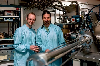
Certain semiconductor structures, so-called quantum dots, might constitute the foundation of quantum communication. They are an efficient interface between matter and light, with photons (light particles) emitted by the quantum dots transporting information across large distances. However, structures form by default during the manufacture of quantum dots that interfere with communication. Researchers at the University of Basel, Ruhr-Universität Bochum, and Forschungszentrum Jülich have now successfully eliminated these interferences. They’ve published their report in the journal Communications Physics from 9 August 2019.
Light Particles Capable of Transporting Information Across Large Distances
Quantum dots can be realised in semiconductors if researchers lock an electron and an electron hole—i.e. a positive charge at a position where an electron should exist—in a constricted space. Together, electron and electron hole form an excited state. When they recombine, the excited state disappears and a photon is generated. “That photon might be usable as information carrier in quantum communication across large distances,” says Dr. Arne Ludwig from the Chair for Applied Solid State Physics in Bochum.
The quantum dots manufactured in Bochum are generated in the semiconductor material indium arsenide. The researchers grow the material on a gallium arsenide substrate. In the process, a smooth indium arsenide layer forms at a thickness of a mere one and a half atomic layers – the so-called wetting layer. Subsequently, the researchers generate small islands with a diameter of 30 nanometres and a height of a few nanometres. These are the quantum dots.
Interfering Photons from Wetting Layer
The wetting layer that has to be deposited in the first step causes problems, because it, too, contains excited electron hole states that decay and may release photons. In the wetting layer, these states decay even more easily than in the quantum dots. The photons emitted in the process can’t be used in quantum communication, however; rather, they generate a static noise in the system.
“The wetting layer covers the entire surface while the quantum dots only cover a thousandth of the semiconductor chip, which is why the interfering light is approximately a thousand times stronger than the light emitted by the quantum dots,” explains Andreas Wieck, Head of the Chair for Applied Solid State Physics in Bochum. “The wetting layer radiates photons at a slightly higher frequency and at a much higher intensity than the quantum dots. It’s as if the quantum dots emitted the chamber pitch A, whereas the wetting layer emitted an B that was a thousand times louder.”
Additional Layer Eliminates Interferences
“We have been able to ignore those interferences by exciting only the required energy states,” says Matthias Löbl from the University of Basel. “However, if quantum dots are to be used as information units for quantum applications, it might be ideal to charge them with more electrons. But in that case, the energy levels in the wetting layer would be likewise excited,” adds Arne Ludwig.
The research team has now eliminated this interference by adding an aluminium arsenide layer grown above the quantum dots in the wetting layer. The energy states in the wetting layer are thus removed, which, in turn, makes it less likely for electrons and electron holes to recombine and emit photons.
Collaboration Between Three Research Institutes
The samples for the current project were generated by Dr. Sven Scholz at the RUB Chair of Applied Solid State Physics, whose work was awarded with the dissertation prize by the Wilhelm and Else Heraeus Foundation in June 2019. The measurements of the size of interferences with and without the aluminium arsenide layer were conducted by the team at the University of Basel, under the auspices of Matthias Löbl, Dr. Immo Söllner and Professor Richard Warburton. The group at Forschungszentrum Jülich captured high-resolution microscope images of the samples.
Share on:


Testimonial
"We’re proud to call I-Connect007 a trusted partner. Their innovative approach and industry insight made our podcast collaboration a success by connecting us with the right audience and delivering real results."
Julia McCaffrey - NCAB GroupSuggested Items
Indium to Highlight Energy-Efficient, High-Reliability Solder Solutions for EV and Electronics at Productronica India
09/03/2025 | Indium CorporationIndium Corporation, a leading materials refiner, smelter, manufacturer, and supplier to the global electronics, semiconductor, electric vehicle (EV), thin-film, and thermal management markets, will feature a range of sustainable, high-reliability solder products at Productronica India, to be held September 17-19 in Bengaluru, India.
Indium Promotes Huang to Senior Manager, Marketing Communications
08/28/2025 | Indium CorporationWith its commitment to innovation and growth through employee development, Indium Corporation announces the promotion of Jingya Huang to Senior Manager, Marketing Communications, to continue to lead the company’s branding and promotional efforts.
Indium Expert to Present on AI Thermal Challenges at INEMI Forum on Complex Integrated Electronics
08/26/2025 | Indium CorporationIndium Corporation Assistant Product Manager Foo Siang Hooi will deliver a technical presentation on addressing thermal challenges in AI and high-performance computing (HPC) with metal-based thermal interface materials (TIMs) at the International Electronics Manufacturing Initiative (INEMI) Forum on Complex Integrated Electronics, to be held September 17-18 in Penang, Malaysia.
Indium Corporation to Showcase Innovative Materials Enabling AI Technology at SEMICON Taiwan
08/20/2025 | Indium CorporationIndium Corporation®, a leading materials refiner, smelter, manufacturer, and supplier to the global electronics, semiconductor, AI, thin-film, and thermal management markets, will showcase its heterogeneous integration and assembly (HIA) products and thermal interface materials (TIMs) at SEMICON Taiwan, to be held September 10-12 in Taipei, Taiwan.
Indium Corporation Promotes Two Leaders in EMEA (Europe, Middle East, and Africa) Markets
08/05/2025 | Indium CorporationWith its commitment to innovation and growth through employee development, Indium Corporation today announced the promotions of Andy Seager to Associate Director, Continental Sales (EMEA), and Karthik Vijay to Senior Technical Manager (EMEA). These advancements reflect their contributions to the company’s continued innovative efforts with customers across Europe, the Middle East, and Africa (EMEA).