


 Flexible Thinking: Designing Flex Circuits for Dynamic Reliability
 Global PCB Connections: Rigid-flex and Flexible PCBs—The Backbone of Modern Electronics
 Happy’s Tech Talk #29: Bend-to-Install Semi-flex FR-4


Lasers Enable Engineers to Weld Ceramics, No Furnace Required
August 26, 2019 | UC San DiegoEstimated reading time: 2 minutes
Smartphones that don’t scratch or shatter. Metal-free pacemakers. Electronics for space and other harsh environments. These could all be made possible thanks to a new ceramic welding technology developed by a team of engineers led by the University of California San Diego.
The process uses an ultrafast pulsed laser to melt ceramic materials along the interface and fuse them together. It works in ambient conditions and uses less than 50 watts of laser power, making it more practical than current ceramic welding methods that require heating the parts in a furnace.
Ceramics have been fundamentally challenging to weld together because they need extremely high temperatures to melt, exposing them to extreme temperature gradients that cause cracking, explained senior author Javier E. Garay, a professor of mechanical engineering and materials science and engineering at UC San Diego, who led the work in collaboration with UC Riverside professor and chair of mechanical engineering Guillermo Aguilar. Ceramic materials are of great interest because they are biocompatible, extremely hard and shatter resistant, making them ideal for biomedical implants and protective casings for electronics. However, current ceramic welding procedures are not conducive to making such devices.
“Right now there is no way to encase or seal electronic components inside ceramics because you would have to put the entire assembly in a furnace, which would end up burning the electronics,” Garay said.
Garay, Aguilar and colleagues’ solution was to aim a series of short laser pulses along the interface between two ceramic parts so that heat builds up only at the interface and causes localized melting. They call their method ultrafast pulsed laser welding.
To make it work, the researchers had to optimize two aspects: the laser parameters (exposure time, number of laser pulses, and duration of pulses) and the transparency of the ceramic material. With the right combination, the laser energy couples strongly to the ceramic, allowing welds to be made using low laser power (less than 50 watts) at room temperature. “The sweet spot of ultrafast pulses was two picoseconds at the high repetition rate of one megahertz, along with a moderate total number of pulses. This maximized the melt diameter, minimized material ablation, and timed cooling just right for the best weld possible,” Aguilar said.
“By focusing the energy right where we want it, we avoid setting up temperature gradients throughout the ceramic, so we can encase temperature-sensitive materials without damaging them,” Garay said.
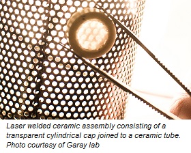
As a proof of concept, the researchers welded a transparent cylindrical cap to the inside of a ceramic tube. Tests showed that the welds are strong enough to hold vacuum.
“The vacuum tests we used on our welds are the same tests that are used in industry to validate seals on electronic and optoelectronic devices,” said first author Elias Penilla, who worked on the project as a postdoctoral researcher in Garay’s research group at UC San Diego.
The process has so far only been used to weld small ceramic parts that are less than two centimeters in size. Future plans will involve optimizing the method for larger scales, as well as for different types of materials and geometries.
Share on:


Testimonial
"The I-Connect007 team is outstanding—kind, responsive, and a true marketing partner. Their design team created fresh, eye-catching ads, and their editorial support polished our content to let our brand shine. Thank you all! "
Sweeney Ng - CEE PCBSuggested Items
AI Demand Drives PCB Material Market Growth
05/08/2026 | TPCAAs AI computing continues to drive a comprehensive upgrade in hardware specifications, the global printed circuit board industry is undergoing a profound structural transformation.
I-Connect007 Editor’s Choice: Five Must-Reads for the Week
05/01/2026 | Michelle Te, I-Connect007If it feels like the PCB industry is accelerating faster than ever, you’re not imagining it. From advanced materials driven by AI applications to renewed investment in domestic manufacturing—and the next generation stepping into critical roles—there’s a lot shifting at once. My selections for this week highlight where the pressure points are forming, and where the opportunities are emerging.
Electronics Manufacturing Needs Your Voice: Global Sentiment Survey Now Live
04/30/2026 | Global Electronics AssociationThe latest monthly Global Sentiment Survey from the Global Electronics Association is now open. At a time when demand uncertainty, policy shifts, energy costs, and supply chain recalibration are pulling the industry in multiple directions, the survey captures something macroeconomic data often misses: how manufacturers are actually experiencing conditions on the ground.
From Backbone to Breakthroughs: I-Connect007 Wraps PCB Materials Series with Focus on Innovation
05/06/2026 | I-Connect007I-Connect007 wraps up its six-part podcast series, PCB Materials: The Backbone and Future of Electronics, with Episode 6 and a discussion focusing on innovation. In Episode 6, Marcy LaRont speaks with Isola CTO Kirk Thompson about a critical turning point for the PCB industry as innovation accelerates. As data rates climb and demands from AI infrastructure, power density, flexible electronics, photonics, and chiplet integration intensify, traditional material assumptions are no longer sufficient.
Jiva Soluboard Getting the Attention It Deserves
04/30/2026 | Marcy LaRont, I-Connect007 MagazineJiva is a newer company that bridges the divide between PCB fabrication and product circularity or sustainability. Jiva Soluboard is the first fully recyclable laminate material ever created for PCB fabrication, and it's not going unnoticed. Stephen Driver, CEO of Jiva, gave us an update at APEX EXPO, including an exciting certification achievement in February.