


 Dan’s Biz Bookshelf: ‘Abundance: How We Build a Better Future’
 Trouble in Your Tank: In Complex Systems, Design Rules Aren’t Optional
 It’s Only Common Sense: The Phone Is Still Your Competitive Advantage


Gallium Oxide Power Transistors with Record Values
August 27, 2019 | Forschungsverbund Berlin e. V.Estimated reading time: 1 minute
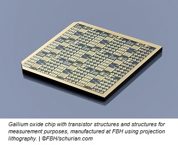
The Ferdinand-Braun-Institut (FBH) has now achieved a breakthrough with transistors based on gallium oxide (ß-Ga2O3).
The newly developed ß-Ga2O3-MOSFETs (metal-oxide-semiconductor field-effect transistor) provide a high breakdown voltage combined with high current conductivity. With a breakdown voltage of 1.8 kilovolts and a record power figure of merit of 155 megawatts per square centimeter, they achieve unique performance figures close to the theoretical material limit of gallium oxide. At the same time, the breakdown field strengths achieved are significantly higher than those of established wide bandgap semiconductors such as silicon carbide or gallium nitride.
On a footprint as small as possible, these MOSFETs should offer low energy consumption and achieve ever higher power densities, thus working more efficiently. This is where conventional devices reach their limits. Scientists all over the world are therefore investigating new materials and components that can meet these requirements.
Optimized Layer Structure and Gate Topology
In order to achieve these improvements, the FBH team tackled the layer structure and gate topology. The basis was provided by substrates from the Leibniz Institute for Crystal Growth with an optimized epitaxial layer structure. As a result, the defect density could be reduced and electrical properties improved. This leads to lower on-state resistances. The gate is the central ‘switching point’ of field effect transistors, controlled by the gate-source voltage. Its topology has been further optimized, allowing to reduce high field strengths at the gate edge. This in turn leads to higher breakdown voltages.
Share on:


Subscribe
Stay ahead of the technologies shaping the future of electronics with our latest newsletter, Advanced Electronics Packaging Digest. Get expert insights on advanced packaging, materials, and system-level innovation, delivered straight to your inbox.
Subscribe now to stay informed, competitive, and connected.
Suggested Items
OKI Develops 180-Layer, 15 mm PCB for AI Semiconductor Test Equipment
04/29/2026 | BUSINESS WIREOKI Circuit Technology, the OKI Group’s printed circuit board (PCB) business company, has successfully developed design and production technologies for 180-layer, 15 mm-thick PCBs intended for use in wafer testing equipment for high bandwidth memory (HBM) mounted on AI semiconductors.
Target Condition: An Exploration of Flooding PCB Layers
04/02/2026 | Kelly Dack -- Column: Target ConditionThe concept of flooding PCB layers with copper has been around for so long, you’d think we’d have it mastered. We haven’t. (Oh, and by “we,” I mean design engineers and the software tools we depend on.) Years ago, PCB artwork was created by hand using light tables, with tape applied to Mylar. Signals were slow, traces were relatively wide, and high-current paths were simply “beefed up” with wider copper. Signal integrity wasn’t yet a driving concern. Today, solid return paths are fundamental to robust design. We understand the importance of continuous reference planes for signal integrity and EMI control.
Happy’s Tech Talk #47: Automation for Complex Multilayer Fabrication Stackups
03/31/2026 | Happy Holden -- Column: Happy’s Tech TalkMultilayer stackups have evolved dramatically as they’ve been adopted for high-performance computing (HPC) and artificial intelligence (AI) server applications. These high-speed, high I/O designs require the designer and fabricator to manage more boundary conditions than ever before. In practice, the stackup is no longer “just a stackup.” It becomes the foundation for signal integrity, reliability, manufacturability, and cost.
SCHMID Group Wins Major Order for Wet-Process Equipment for AI & HPC Infrastructure
03/11/2026 | SCHMID GroupSCHMID Group, a leading global supplier of advanced wet process equipment for the electronics manufacturing industry, has secured a lower two-digit million-USD purchase order from a major Asian high-end PCB manufacturer for a new HDI multilayer production line.
Standard of Excellence: Building the Board of the Future—Materials, Methods, and Mindset
02/18/2026 | Anaya Vardya -- Column: Standard of ExcellenceThe future of PCB manufacturing is here. The products we’re being asked to build today would have been called “advanced” just a few years ago. What was once special is now standard, and what was once impossible is now expected. The challenge and the opportunity lie in leading the charge to the next frontier of printed circuit board design, materials, and manufacturing discipline. To build the board of the future, we need new materials, smarter methods, and a mindset of innovation anchored in flawless execution.