


 Punching Out: How to Stay Focused in Business and M&A
 It’s Only Common Sense: Just Imagine…
 Marcy’s Musings: Old School vs. New School—When Does It Matter?


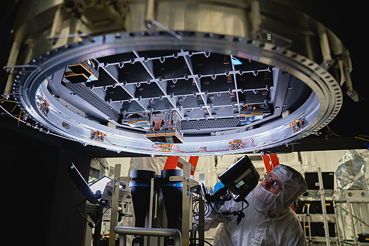
After 16 years of dedicated planning and engineering, scientists at the U.S. Department of Energy’s (DOE) Brookhaven National Laboratory have completed a 3.2 gigapixel sensor array for the camera that will be used in the Large Synoptic Survey Telescope (LSST), a massive telescope that will observe the universe like never before.
“This is the biggest charge-coupled device (CCD) array that has ever been built,” said Paul O’Connor, senior scientist at Brookhaven Lab’s instrumentation division. “It’s three billion pixels. No telescope has ever put this many sensors into one camera.”
The digital sensor array is composed of about 200 16-megapixel sensors, divided into 21 modules called “rafts.” Each raft can function on its own, but when combined, they will view an area of sky that can fit more than 40 full moons in a single image. Researchers will stitch these images together to create a time-lapse movie of the complete visible universe accessible from Chile.
Currently under construction on a mountaintop in Chile, LSST is designed to capture the most complete images of our universe that have ever been achieved. The project to build the telescope facility and camera is a collaborative effort among more than 30 institutions from around the world, and it is primarily funded by DOE’s Office of Science and the National Science Foundation. DOE’s SLAC National Accelerator Laboratory is leading the overall effort to construct the camera—the world’s largest camera for astronomy—while Brookhaven led the design, construction, and qualification of the digital sensor array—the “digital film” for the camera.
“It’s the heart of the camera,” said Bill Wahl, science raft subsystem manager of the LSST project at Brookhaven Lab. “What we’ve done here at Brookhaven represents years of great work by many talented scientists, engineers, and technicians. Their work will lead to a collection of images that has never been seen before by anyone. It’s an exciting time for the project and for the Lab.”
Members of the LSST project team at Brookhaven Lab are shown with a prototype raft cryostat. In addition to the rafts, Brookhaven scientists designed and built the cryostats that hold and cool the rafts to -100° Celsius. Pictured from left to right are Sean Robinson, Michael Keach, Matthew Rumore, Gabriella Carini, Steven Andrade, Colleen Michael, Veljko Radeka, Wendy Morrin, Bill Wahl, Phil Kuczewski, HyeYun Park, Ivan Kotov, Andrei Nomerotski, Justine Haupt, Alfred Dellapenna, Connor Miraval, Sven Herrmann, Brian Walsh, Steve Bellavia, Paul Stankus, and Paul O'Connor. Team members not pictured include Peter Takacs, Michelle McQueen, John Kuczewski, Steve Plate, Paul Palecek, Rebecca Coles, Jason Farrell, Raj Gutta, Elliott Golnar, Anze Slozar, Don Elliott, Ron Angona, August Hoffman, David Asner, Graham Smith, and Kurt Vetter.
Page 1 of 2


