


 Dan’s Biz Bookshelf: ‘Abundance: How We Build a Better Future’
 Trouble in Your Tank: In Complex Systems, Design Rules Aren’t Optional
 It’s Only Common Sense: The Phone Is Still Your Competitive Advantage


Researchers Demonstrate First All-Metamaterial Optical Gas Sensor
September 3, 2019 | OSAEstimated reading time: 3 minutes
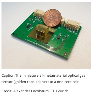
Researchers have developed the first fully-integrated, non-dispersive infrared (NDIR) gas sensor enabled by specially engineered synthetic materials known as metamaterials. The sensor has no moving parts, requires little energy to operate and is among the smallest NDIR sensors ever created.
The sensor is ideal for new Internet of Things and smart home devices designed to detect and respond to changes in the environment. It also could find use in future medical diagnostics and monitoring equipment.
“Our sensor design unites simplicity, robustness, and efficiency. Using metamaterials, we can omit one of the main cost drivers in NDIR gas sensors, the dielectric filter, and simultaneously reduce the size and energy consumption of the device,” said Alexander Lochbaum from the Institute of Electromagnetic Fields of ETH Zurich, Switzerland, and lead author on the paper. “This makes the sensors viable for high-volume, low-cost markets such as automotive and consumer electronics.”
NDIR sensors are among the commercially most relevant types of optical gas sensors, used to assess vehicle exhaust, measure air quality, detect gas leaks and support a variety of medical, industrial and research applications. The new sensor’s small size, potentially low cost, and reduced energy requirements open new opportunities for these and other types of applications.
Shrinking the Optical Pathway
Conventional NDIR sensors work by shining infrared light through air in a chamber until it reaches a detector. An optical filter positioned in front of the detector eliminates all light except the wavelength that is absorbed by a particular gas molecule so that the amount of light entering the detector indicates the concentration of that gas in the air. Though most NDIR sensors measure carbon dioxide, different optical filters can be used to measure a wide range of other gases.
In recent years, engineers have replaced the conventional infrared light source and detector with microelectromechanical systems (MEMS) technology, miniscule components that bridge between mechanical and electrical signals. In the new work, researchers integrate metamaterials onto a MEMS platform to further miniaturize the NDIR sensor and dramatically enhance the optical path length.
Key to the design is a type of metamaterial known as a metamaterial perfect absorber (MPA) made from a complex layered arrangement of copper and aluminum oxide. Because of its structure, MPA can absorb light coming from any angle. To take advantage of this, the researchers designed a multi-reflective cell that “folds” the infrared light by reflecting it many times over. This design allowed a light absorption path about 50 millimeters long to be squeezed into a space measuring only 5.7 × 5.7 × 4.5 millimeters.
Whereas conventional NDIR sensors require light to pass through a chamber a few centimeters long to detect gas at very low concentrations, the new design optimizes light reflection to accomplish the same level of sensitivity in a cavity that is just over half a centimeter long.
A Simple, Robust, And Low-Cost Sensor
By using metamaterials for efficient filtering and absorption, the new design is both simpler and more robust than existing sensor designs. Its main parts are a metamaterial thermal emitter, an absorption cell, and a metamaterial thermopile detector. A microcontroller periodically heats up the hotplate, causing the metamaterial thermal emitter to generate infrared light. The light travels through the absorption cell and is detected by the thermopile. The microcontroller then collects the electronic signal from the thermopile, and streams the data to a computer.
The primary energy requirement comes from the power needed to heat the thermal emitter. Thanks to the high efficiency of the metamaterial used in the thermal emitter, the system works at much lower temperatures than previous designs, so less energy is needed for each measurement.
The researchers tested the device’s sensitivity by using it to measure varying concentrations of carbon dioxide in a controlled atmosphere. They demonstrated it can detect carbon dioxide concentrations with a noise-limited resolution of 23.3 parts per million, a level on par with commercially available systems. However, to do this the sensor required only 58.6 millijoules of energy per measurement, about a five-fold reduction compared to commercially available low-power thermal NDIR carbon dioxide sensors.
“For the first time, we realize an integrated NDIR sensor that relies exclusively on metamaterials for spectral filtering. Applying metamaterial technology for NDIR gas sensing allows us to rethink the optical design of our sensor radically, leading to a more compact and robust device,” said Lochbaum.
About The Optical Society
Founded in 1916, The Optical Society (OSA) is the leading professional organization for scientists, engineers, students and business leaders who fuel discoveries, shape real-life applications and accelerate achievements in the science of light. Through world-renowned publications, meetings and membership initiatives, OSA provides quality research, inspired interactions and dedicated resources for its extensive global network of optics and photonics experts. For more information, visit osa.org.
Share on:


Subscribe
Stay ahead of the technologies shaping the future of electronics with our latest newsletter, Advanced Electronics Packaging Digest. Get expert insights on advanced packaging, materials, and system-level innovation, delivered straight to your inbox.
Subscribe now to stay informed, competitive, and connected.
Suggested Items
Driving Innovation: Selecting the Right Laser Source
04/28/2026 | Simon Khesin -- Column: Driving InnovationWhen I first joined Schmoll Maschinen, I brought experience from almost every PCB process, except for laser. As I immersed myself in laser processing, I realized why it can seem so daunting to a newcomer. The complexity arises from three intersecting factors: A vast variety of laser sources: CO2, UV-nano, green-pico, UV-pico, IR-pico, and others; a diverse range of applications: Drilling, cutting, ablation, and more; and an extensive list of materials: These have vastly different absorption rates. Choosing the right machine or laser source is rarely trivial. Even for experienced engineers, answering "Which source is best?" requires examining the business's specific goals.
Institute of Circuit Technology Spring Seminar 2026: A Bright Future in Europe
04/23/2026 | Pete Starkey, I-Connect007Through the leafy lanes and spring flowers of Warwickshire and back to Meridan, the traditional centre of England, and now officially part of the Metropolitan Borough of Solihull in the county of the West Midlands, I attended the Annual General Meeting and Spring Seminar of the Institute of Circuit Technology (ICT) on April 14. Out of the AGM came notable changes in leadership at the top of the Institute: the retirement of Mat Beadel as chair and Emma Hudson as technical director. Effective May 1, Steve Driver is the new chair, and Alun Morgan is the new technical director.
ACCM Unveils Negative and Near-zero CTE Materials for Large-Format AI Chips
04/21/2026 | Advanced Chip and Circuit MaterialsAdvanced Chip and Circuit Materials, Inc. (ACCM) has launched two new materials: Celeritas HM50, with a negative coefficient of thermal expansion (CTE) of -8 ppm/°C to offset the positive CTE and expansion of copper with temperature on circuit boards, and Celeritas HM001, with near-zero CTE and the low-loss performance needed for high-speed signal layers to 224 Gb/s and faster in artificial intelligence (AI) circuits.
Fresh PCB Concepts: Designing PCBs for Harsh Environments—Reliability Is Engineered Upstream
04/23/2026 | Team NCAB -- Column: Fresh PCB ConceptsWhen engineers hear the phrase “harsh environment,” they usually think of the extreme temperature swings, vibration and shock, pressure changes, or radiation in aerospace. However, aerospace is not the only harsh environment where electronic assemblies must survive. Automotive power electronics, downhole oil and gas tools, marine controls, rail systems, defense platforms, and industrial automation equipment all expose PCBs to environments that are equally unforgiving. The stress mechanisms may differ, but the physics does not.
Advanced Packaging for AI: Reliability Starts at the Cu/Cu/Cu Microvia Junction
04/20/2026 | Kuldip Johal, MKS' AtotechThe rapid growth of AI computing, from training clusters to inference at scale, is reshaping demand across the entire electronics supply chain. Advances in technology requirements, such as higher bandwidth, lower latency, and greater compute density, are driving the development of advanced packaging technologies and transforming the PCB industry across design, manufacturing, testing, and even architecture.