


 The Right Approach: Get Ready for ISO 9001 Version 6
 Dan’s Biz Bookshelf: ‘Still Broke: Walmart’s Remarkable Transformation'
 Driving Innovation: Depth Routing Processes—Achieving Unparalleled Precision in Complex PCBs


New Insulation Technique Paves the Way for More Powerful and Smaller Chips
September 5, 2019 | KU LeuvenEstimated reading time: 2 minutes
Researchers at KU Leuven and imec have successfully developed a new technique to insulate microchips. The technique uses metal-organic frameworks, a new type of materials consisting of structured nanopores. In the long term, this method can be used for the development of even smaller and more powerful chips that consume less energy. The team has received an ERC Proof of Concept grant to further their research.
Computer chips are getting increasingly smaller. That’s not new: Gordon Moore, one of the founders of chip manufacturer Intel, already predicted it in 1965. Moore's law states that the number of transistors in a chip, or integrated circuit, doubles about every two years. This prognosis was later adjusted to 18 months, but the theory still stands. Chips are getting smaller and their processing power is increasing. Nowadays, a chip can have over a billion transistors.
But this continued reduction in size also brings with it a number of obstacles. The switches and wires are packed together so tightly that they generate more resistance. This, in turn, causes the chip to consume more energy to send signals. To have a well-functioning chip, you need an insulating substance that separates the wires from each other, and ensures that the electrical signals are not disrupted. However, that’s not an easy thing to achieve at the nanoscale level.
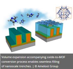
A study led by KU Leuven professor Rob Ameloot (Department of Microbial and Molecular systems) shows that a new technique might provide the solution. “We’re using metal-organic frameworks (MOFs) as the insulating substance. These are materials that consist of metal ions and organic molecules. Together, they form a crystal that is porous yet sturdy.”
For the first time, a research team at KU Leuven and imec managed to apply the MOF insulation to electronic material. An industrial method called chemical vapour deposition was used for this, says postdoctoral researcher Mikhail Krishtab (Department of Microbial and Molecular systems). “First, we place an oxide film on the surface. Then, we let it react with vapour of the organic material. This reaction causes the material to expand, forming the nanoporous crystals.”
“The main advantage of this method is that it's bottom-up,” says Krishtab. “We first deposit an oxide film, which then swells up to a very porous MOF material. You can compare it to a soufflé that puffs up in the oven and becomes very light. The MOF material forms a porous structure that fills all the gaps between the conductors. That’s how we know the insulation is complete and homogeneous. With other, top-down methods, there's always still the risk of small gaps in the insulation.”
Share on:


Testimonial
"Advertising in PCB007 Magazine has been a great way to showcase our bare board testers to the right audience. The I-Connect007 team makes the process smooth and professional. We’re proud to be featured in such a trusted publication."
Klaus Koziol - atgSuggested Items
Meet the Author Podcast: Martyn Gaudion Unpacks the Secrets of High-Speed PCB Design
07/16/2025 | I-Connect007In this special Meet the Author episode of the On the Line with… podcast, Nolan Johnson sits down with Martyn Gaudion, signal integrity expert, managing director of Polar Instruments, and three-time author in I-Connect007’s popular The Printed Circuit Designer’s Guide to... series.
Intervala Hosts Employee Car and Motorcycle Show, Benefit Nonprofits
08/27/2024 | IntervalaIntervala hosted an employee car and motorcycle show, aptly named the Vala-Cruise and it was a roaring success! Employees had the chance to show off their prized wheels, and it was incredible to see the variety and passion on display.
KIC Honored with IPC Recognition for 25 Years of Membership and Contributions to Electronics Manufacturing Industry
06/24/2024 | KICKIC, a renowned pioneer in thermal process and temperature measurement solutions for electronics manufacturing, is proud to announce that it has been recognized by IPC for 25 years of membership and significant contributions to electronics manufacturing.
Boeing Starliner Spacecraft Completes Successful Crewed Docking with International Space Station
06/07/2024 | BoeingNASA astronauts Barry "Butch" Wilmore and Sunita "Suni" Williams successfully docked Boeing's Starliner spacecraft to the International Space Station (ISS), about 26 hours after launching from Cape Canaveral Space Force Station.
KIC’s Miles Moreau to Present Profiling Basics and Best Practices at SMTA Wisconsin Chapter PCBA Profile Workshop
01/25/2024 | KICKIC, a renowned pioneer in thermal process and temperature measurement solutions for electronics manufacturing, announces that Miles Moreau, General Manager, will be a featured speaker at the SMTA Wisconsin Chapter In-Person PCBA Profile Workshop.