


 Trouble in Your Tank: Implementing Direct Metallization in Advanced Substrate Packaging
 It’s Only Common Sense: Storytelling That Sells—Stop Pitching, Start Painting Pictures
 The Right Approach: Get Ready for ISO 9001 Version 6


EIPC Summer Conference 2019, Day 1
September 10, 2019 | Alun Morgan, EIPCEstimated reading time: 14 minutes
Continuing with the inkjet theme, the conference wouldn’t be complete without hearing from Don Monn of Taiyo who didn’t disappoint with his presentation on white solder mask for automotive applications. He started with an estimate of the automotive lighting market value, which was US$25.7B in 2016 and will rise to US$35.9B by 2022. Then, Monn explained the requirement for white solder mask in automotive lighting with details of the stringent specifications for gloss, reflectance, and colour stability after thermal ageing. He also addressed the challenges of producing a highly opaque material that had high-enough photosensitivity to offer a wide process window.
Monn went on to explain that cracking is more prevalent in white solder mask than standard green solder mask during assembly and the reasons behind this before introducing Taiyo’s new white solder mask, which was specifically designed to reduce the challenges of cracking and photosensitivity without compromising other essential properties. In addition to the general requirements, Monn shared additional specifications for ionic contamination, hot storage, and solvent resistance along with the test results for the Taiyo product showing that all requirements were fully achieved.
Closing the session and the first day of the conference was David Bernard of David Bernard Consultancy, whose presentation was entitled “Bare Board Inspection: Ensuring a Sound Foundation for Assembly.” He began by explaining how PCB assemblers had long used X-ray inspection techniques driven by the need to inspect optically hidden joints. X-ray systems offering high-magnification, high-resolution imaging provided top-down and oblique angle views. Considering the difficulties faced in checking bare boards before assembly, Bernard introduced the concept of using the PCB assembler’s existing X-ray equipment to provide quick, non-destructive tests on representative samples of bare boards.
To demonstrate this concept, Bernard showed oblique X-ray images with impressive examples of poor drilling quality, layer misalignment, plating failure, and cracks. Moving on from the 2D examples, he showed partial computed tomography (PCT) images where the benefits of reconstructed 2D X-ray slices at different levels in the Z-direction with a decluttered image allowing individual layers to be analysed were readily apparent. Bernard described the PCT technique as being able to be undertaken anywhere on the board non-destructively, whilst full CT, which is destructive, requires a small volume (like that used for micro-section) to enable high-magnification/high-resolution 3D models. Bernard concluded by stating that there is a place for all of the described techniques and suggested that they are used in this order: 2D views, then PCT, full CT, and micro-section.
Tour and Dinner
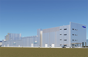
Before departing for the bonus programme visit to AT&S, Jürgen Deutschmann gave an informative presentation. He explained that although AT&S is headquartered in Austria, it operates six manufacturing plants in Europe and Asia with 10,000 employees. In addition to being among the top 10 PCB producers worldwide, AT&S also holds the third position globally in high-end technology. Deutschmann then identified R&D as the key for technological leadership and informed the audience that over 40% of revenue is generated with products that had new and innovative technologies introduced to the market within the last three years.
After a safety briefing, AT&S hosted a tour of its Leoben facility, which was impeccably clean, well-organised, and highly automated. Delegates were highly impressed at the level of technology in the plant and professionalism that was shown by the AT&S guides and were very grateful for their kind hospitality.
Following the AT&S tour, the delegates were invited for dinner at Gösserbräu in Leoben where the EIPC staff were, once again, surprised to find that a brewery made an excellent networking venue. The beer and food were excellent, but I most highly appreciated the quality of the company. Daniel Geiger graciously joined us for dinner and very kindly requisitioned some local buses to take us back to the hotel.
Look for Part 2 of this coverage coming soon.
Technical editor’s note: I most gratefully acknowledge the support of EIPC Chairman Alun Morgan for preparing this review and providing the photographs. Many thanks! —Pete Starkey
Page 3 of 3Share on:


Testimonial
"In a year when every marketing dollar mattered, I chose to keep I-Connect007 in our 2025 plan. Their commitment to high-quality, insightful content aligns with Koh Young’s values and helps readers navigate a changing industry. "
Brent Fischthal - Koh YoungSuggested Items
Koh Young, Fuji, and Kurtz ERSA Drive Smart Manufacturing Solutions for EV and Automotive Electronics at Kunshan, China Technical Seminar
09/11/2025 | Koh YoungKoh Young Technology, the global leader in True 3D measurement-based inspection solutions, partnered with Fuji Corporation and Kurtz ERSA to host an exclusive technical seminar for leading automotive manufacturers in East China. Held on September 4 at Fuji’s factory in Kunshan, the event gathered participants representing over 35 companies.
MacDermid Alpha Presents at SMTA New Delhi, Bangalore Chapter, on Flux–OSP Interaction
09/09/2025 | MacDermid Alpha Electronics SolutionsMacDermid Alpha contributes technical insights on OSP solderability at the Bangalore Chapter, SMTA reinforcing commitment to knowledge-sharing and industry collaboration.
Electra’s ElectraJet EMJ110 Inkjet Soldermask Now in Black & Blue at Sunrise Electronics
09/08/2025 | Electra Polymers LtdFollowing the successful deployment of Electra’s Green EMJ110 Inkjet Soldermask on KLA’s Orbotech Neos™ platform at Sunrise Electronics in Elk Grove Village, Illinois, production has now moved beyond green.
Absolute EMS: The Science of the Perfect Solder Joint
09/05/2025 | Absolute EMS, Inc.Absolute EMS, Inc., a six-time award-winning provider of fast turnaround, turnkey contract electronic manufacturing services (EMS), is drawing attention to the critical role of 3D Solder Paste Inspection (SPI) in ensuring the reliability of both FLEX and rigid printed circuit board assemblies (PCBAs).
Indium Corporation to Highlight High-Reliability Solder Solutions at SMTA Guadalajara Expo
09/04/2025 | Indium CorporationIndium Corporation, a leading materials refiner, smelter, manufacturer, and supplier to the global electronics, semiconductor, thin-film, and thermal management markets, will feature a range of innovative, high-reliability solder products for printed circuit board assembly (PCBA) at the SMTA Guadalajara Expo and Tech Forum, to be held September 17-18 in Guadalajara, Mexico.