


 The Right Approach: Get Ready for ISO 9001 Version 6
 Dan’s Biz Bookshelf: ‘Still Broke: Walmart’s Remarkable Transformation'
 Driving Innovation: Depth Routing Processes—Achieving Unparalleled Precision in Complex PCBs


Getting a Look Under the Hood of Topological Insulators
September 11, 2019 | Argonne National LaboratoryEstimated reading time: 2 minutes
Certain materials, like copper, conduct electricity very well. Other materials, like glass, do not. A certain kind of material, called a topological insulator, acts partially like one and partially like the other ― it behaves like a conductor at its surface and an insulator in its interior.
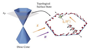
Image Caption: The specific relation between electronic states in a topological insulator and momentum leads to an asymmetric accumulation of spin, depicted on the right, which gives rise to an electric current to second order in an applied electric field E. (Image by Shulei Zhang / Argonne National Laboratory.)
Because of topological insulators’ unique electronic properties and their potential use in spintronic devices and even conceivably as transistors for quantum computers, scientists at the U.S. Department of Energy’s (DOE) Argonne National Laboratory are interested in investigating the special relationship between two properties of the conducting surface electrons in these materials.
In topological insulators, the spin and momentum of each surface electrons are so closely tied that, in scientific parlance, they are locked to one another. “Spin-momentum locking is like having a basketball that must rotate in a specific direction depending on its trajectory down the court,” said Argonne materials scientist Olle Heinonen. “Because an electron also carries a magnetic moment, you can use spin-momentum locking to manipulate magnetic systems very efficiently.”
The electronic structure of topological insulators, including the specifics of spin-momentum locking, may be reflected in the transport behavior of electrons in the materials. To explore the novel behavior of electrons in the topological materials, Argonne scientists worked with scientists at the National University of Singapore, who performed a transport experiment that provided a new perspective of the topologically protected electronic structure.
Heinonen and former Argonne postdoctoral researcher Shulei Zhang described how in the transport experiment a magnetic field applied in the plane of a thin film of a topological insulator can create a voltage in the direction perpendicular to the applied electric current — a phenomenon called a nonlinear planar Hall effect. By varying the direction and intensity of the magnetic field, the Argonne researchers and their colleagues could ascertain from the resulting resistance information as to how the electrons are distributed in terms of their momenta and spin.
“If you know how magnetic fields applied in different directions would affect the nonlinear Hall current measured, you can use our theoretical model to map out how the electrons’ momenta and spins are distributed,” Zhang said. “Then, because of the way we can see more precisely how the electromagnetic fields interact with the surface conduction electrons, we can get much more detailed information of the surface electronic structure of topological insulators.”
The tie between the nonlinear planar Hall effect and the topological surface states with spin-momentum locking is, according to Heinonen, a “macroscopic-microscopic relationship.” “It really gives us a look under the hood,” he said.
A paper based on the study, “Nonlinear planar hall effect,” appeared in the July 1 online edition of Physical Review Letters.
Researchers from the University of Missouri also collaborated on the work. Funding for the study came from DOE’s Office of Science (Office of Basic Energy Sciences).
Share on:


Testimonial
"The I-Connect007 team is outstanding—kind, responsive, and a true marketing partner. Their design team created fresh, eye-catching ads, and their editorial support polished our content to let our brand shine. Thank you all! "
Sweeney Ng - CEE PCBSuggested Items
Closing the Loop on PCB Etching Waste
09/09/2025 | Shawn Stone, IECAs the PCB industry continues its push toward greener, more cost-efficient operations, Sigma Engineering’s Mecer System offers a comprehensive solution to two of the industry’s most persistent pain points: etchant consumption and rinse water waste. Designed as a modular, fully automated platform, the Mecer System regenerates spent copper etchants—both alkaline and acidic—and simultaneously recycles rinse water, transforming a traditionally linear chemical process into a closed-loop system.
Driving Innovation: Depth Routing Processes—Achieving Unparalleled Precision in Complex PCBs
09/08/2025 | Kurt Palmer -- Column: Driving InnovationIn PCB manufacturing, the demand for increasingly complex and miniaturized designs continually pushes the boundaries of traditional fabrication methods, including depth routing. Success in these applications demands not only on robust machinery but also sophisticated control functions. PCB manufacturers rely on advanced machine features and process methodologies to meet their precise depth routing goals. Here, I’ll explore some crucial functions that empower manufacturers to master complex depth routing challenges.
Trouble in Your Tank: Minimizing Small-via Defects for High-reliability PCBs
08/27/2025 | Michael Carano -- Column: Trouble in Your TankTo quote the comedian Stephen Wright, “If at first you don’t succeed, then skydiving is not for you.” That can be the battle cry when you find that only small-diameter vias are exhibiting voids. Why are small holes more prone to voids than larger vias when processed through electroless copper? There are several reasons.
The Government Circuit: Navigating New Trade Headwinds and New Partnerships
08/25/2025 | Chris Mitchell -- Column: The Government CircuitAs global trade winds continue to howl, the electronics manufacturing industry finds itself at a critical juncture. After months of warnings, the U.S. Government has implemented a broad array of tariff increases, with fresh duties hitting copper-based products, semiconductors, and imports from many nations. On the positive side, tentative trade agreements with Europe, China, Japan, and other nations are providing at least some clarity and counterbalance.
How Good Design Enables Sustainable PCBs
08/21/2025 | Gerry Partida, Summit InterconnectSustainability has become a key focus for PCB companies seeking to reduce waste, conserve energy, and optimize resources. While many discussions on sustainability center around materials or energy-efficient processes, PCB design is an often overlooked factor that lies at the heart of manufacturing. Good design practices, especially those based on established IPC standards, play a central role in enabling sustainable PCB production. By ensuring designs are manufacturable and reliable, engineers can significantly reduce the environmental impact of their products.