


 The Right Approach: Get Ready for ISO 9001 Version 6
 Dan’s Biz Bookshelf: ‘Still Broke: Walmart’s Remarkable Transformation'
 Driving Innovation: Depth Routing Processes—Achieving Unparalleled Precision in Complex PCBs


Multimaterial Fiber “Ink” for 3-D-Printed Devices
September 12, 2019 | MITEstimated reading time: 4 minutes
A new method developed by MIT researchers uses standard 3-D printers to produce functioning devices with the electronics already embedded inside. The devices are made of fibers containing multiple interconnected materials, which can light up, sense their surroundings, store energy, or perform other actions.
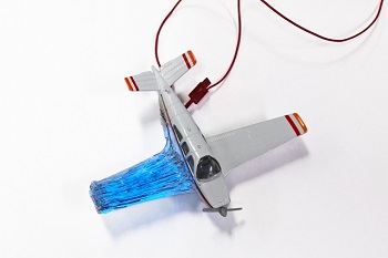
Image Caption: Using the 3D printing method developed by the MIT researchers, a structure such as this model airplane wing could have both light emitters and light detectors embedded in the material, so that it could continuously detect any micro-cracks as they begin to form. Image: Felice Frankel
The new 3-D printing method is described in the journal Nature Communication, in a paper by MIT doctoral student Gabriel Loke, professors John Joannopoulos and Yoel Fink, and four others at MIT and elsewhere.
The system makes use of conventional 3-D printers outfitted with a special nozzle and a new kind of filament to replace the usual single-material polymer filament, which typically gets fully melted before it’s extruded from the printer’s nozzle. The researchers’ new filament has a complex internal structure made up of different materials arranged in a precise configuration, and is surrounded by polymer cladding on the outside.
In the new printer, the nozzle operates at a lower temperature and pulls the filament through faster conventional printers do, so that only its outer layer gets partially molten. The interior stays cool and solid, with its embedded electronic functions unaffected. In this way, the surface is melted just enough to make it adhere solidly to adjacent filaments during the printing process, to produce a sturdy 3-D structure.
The internal components in the filament include metal wires that serve as conductors, semiconductors that can be used to control active functions, and polymer insulators to prevent wires from contacting each other. As a demonstration, the team printed a wing for a model airplane, using filaments that contained both light-emitting and light-detecting electronics. These components could potentially reveal the formation of any microscopic cracks that might develop.
While the filaments used in the model wing contained eight different materials, Loke says that in principle they could contain even more. Until this work, he says, “a printer capable of depositing metals, semiconductors, and polymers in a single platform still did not exist, because printing each of these materials requires different hardware and techniques.”
This method is up to three times faster than any other current approach to fabricating 3-D devices, Loke says, and as with all 3-D printers, offers much more flexibility regarding the kinds of forms that can be produced than typical manufacturing methods do. “Unique to 3-D printing, this approach is able to construct devices of any freeform shapes, which are not achievable by any other methods thus far,” he says.
The method makes use of thermally drawn fibers that contain a variety of different materials embedded within them, a process that Fink and his collaborators have been perfecting for two decades. They have created an array of fibers that have electronic components within them, making the fibers able to carry out a variety of functions. For example, for communications applications, flashing lights can transmit data that is then picked up by other fibers containing light sensors. This approach has for the first time produced fibers, and fabrics woven from them, that have these functions built in.
Now, this new process makes this whole family of fibers available as the raw material for producing functional 3-D devices that can sense, communicate, or store energy, among other actions.
To make the fibers themselves, the different materials are initially assembled into a larger-scale version called a preform, which is then heated and drawn in a furnace to produce a very narrow fiber that contains all those materials, in their same exact relative positions but greatly reduced in size.
The method could potentially be developed further to produce a variety of different kinds of devices, especially for applications where the ability to precisely customize each device is essential. One such area is for biomedical devices, where matching the device to the patient’s own body can be important, says Fink, who is a professor of materials science as well as of electrical engineering and computer science and the CEO of the nonprofit Advanced Functional Fabrics of America.
For example, prosthetic limbs might someday be printed using this method, not only matching the precise dimensions and contours of the patient’s limb, but with all the electronics to monitor and control the limb embedded in place.
Over the years, the group has developed a wide array of fibers containing different materials and functionalities. Loke says virtually all of these can be adapted for the new 3-D-printing technique, making it possible to print objects with a wide variety of different combinations of materials and functions. The device makes use of a standard type of 3-D printer known as a fused deposition modeling (FDM) printer, which is already found in many labs, offices, and even homes.
One application that may be possible in the future would be to print materials for biomedical implants that would provide a scaffolding for the growth of new cells to replace a damaged organ, and include within it sensors to monitor the progress of that growth.
The new method could also be useful for prototyping of devices — already a major application for 3-D printing, but in this case the prototypes would have actual functionality, rather than being static models.
The research team included MIT graduate student Rodger Yuan; former MIT graduate student Michael Rein, who now works at AFFOA; postdoc Tural Khudiyev, and undergraduate student Yash Jain at Stony Brook University in New York. The work was partly supported by the National Science Foundation, the U.S. Army Research Laboratory and the U.S. Army Research Office through the Institute for Soldier Nanotechnologies.
Share on:


Testimonial
"In a year when every marketing dollar mattered, I chose to keep I-Connect007 in our 2025 plan. Their commitment to high-quality, insightful content aligns with Koh Young’s values and helps readers navigate a changing industry. "
Brent Fischthal - Koh YoungSuggested Items
Fresh PCB Concepts: Designing for Success at the Rigid-flex Transition Area
08/28/2025 | Team NCAB -- Column: Fresh PCB ConceptsRigid-flex PCBs come in all shapes and sizes. Manufacturers typically use fire-retardant, grade 4 (FR-4) materials in the rigid section and flexible polyimide materials in the flex region. Because of the small size, some rigid-flex PCBs, like those for hearing aid devices, are among the most challenging to manufacture. However, regardless of its size, we should not neglect the transition area between the rigid and flexible material.
Global Sourcing Spotlight: How to Evaluate Supplier Capabilities Worldwide
08/20/2025 | Bob Duke -- Column: Global Sourcing SpotlightIn global sourcing, the difference between a competitive edge and a catastrophic disruption often comes down to how well you vet your suppliers. Sourcing advanced PCBs, precision components, or materials for complex assemblies demands diligence, skepticism, and more than a little time on airplanes. Here’s how to do your due diligence when evaluating international suppliers and why cutting corners can cost you more than money.
Insulectro and Electroninks Sign North American Distribution Agreement
08/12/2025 | InsulectroElectroninks, a leader in metal organic decomposition (MOD) inks for additive manufacturing and advanced semiconductor packaging, today announced a strategic collaboration and distribution partnership with Insulectro, a premier distributor of materials used in printed electronics and advanced interconnect manufacturing.
Happy’s Tech Talk #41: Sustainability and Circularity for Electronics Manufacturing
08/13/2025 | Happy Holden -- Column: Happy’s Tech TalkI attended INEMI’s June 12 online seminar, “Sustainable Electronics Tech Topic Series: PCBs and Sustainability.” Dr. Maarten Cauwe of imec spoke on “Life Cycle Inventory (LCI) Models for Assessing and Improving the Environmental Impact of PCB Assemblies,” and Jack Herring of Jiva Materials Ltd. spoke on “Transforming Electronics with Recyclable PCB Technology.” This column will review information and provide analysis from both presentations.
Dymax Renews Connecticut Headquarters Lease, Reinforces Long-Term Commitment to Local Community
08/08/2025 | DymaxDymax, a global manufacturer of rapid light-curing materials and equipment, is pleased to announce the renewal and extension of its corporate lease at its 318 Industrial Lane, Torrington, headquarters.