


 The Right Approach: Get Ready for ISO 9001 Version 6
 Dan’s Biz Bookshelf: ‘Still Broke: Walmart’s Remarkable Transformation'
 Driving Innovation: Depth Routing Processes—Achieving Unparalleled Precision in Complex PCBs


Seeing Infrared: Sandia’s Nanoantennas Help Detectors See More Heat, Less Noise
September 17, 2019 | Sandia National LaboratoriesEstimated reading time: 3 minutes
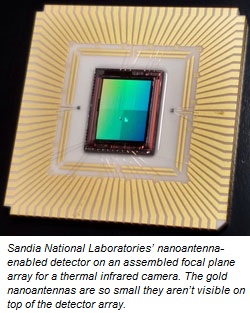
Sandia National Laboratories researchers have developed tiny, gold antennas to help cameras and sensors that “see” heat deliver clearer pictures of thermal infrared radiation for everything from stars and galaxies to people, buildings and items requiring security.
In a Laboratory Directed Research and Development project, a team of researchers developed a nanoantenna-enabled detector that can boost the signal of a thermal infrared camera by up to three times and improve image quality by reducing dark current, a major component of image noise, by 10 to 100 times.
Thermal infrared cameras and sensors have existed for 50 years, but the traditional design of the detector that sits behind the camera lens or a sensor’s optical system seems to be reaching its performance limits, said David Peters, a Sandia manager and nanoantenna project lead.
He said improved sensitivity in infrared detectors, beyond what the typical design can deliver, is important for both Sandia’s national security work and for other uses, such as astronomical research.
Seeing More with Less
The sensitivity and image quality of an infrared detector usually depends on a thick layer of detector material that absorbs incoming heat and turns it into an electrical signal that can be collected and turned into an image. The thickness of the detector layer determines how much heat can be absorbed and read by the camera, but thick layers also have drawbacks.
“The detector material is always spontaneously creating electrons that are collected and add noise to the image, which reduces image quality,” Peters said. “This phenomenon, called dark current, increases along with the thickness of the detector material — the thicker the material is, the more noise in the image it creates.”
The research team developed a new detector design that breaks away from relying on thick layers and instead uses a subwavelength nanoantenna, a patterned array of gold square or cross shapes, to concentrate the light on a thinner layer of detector material. This design uses just a fraction of a micron of detector material, whereas traditional thermal infrared detectors have a thickness of 5 to 10 microns. A human hair is about 75 microns in width.
The nanoantenna-enhanced design helps detectors see more than 50% of an object’s infrared radiation while also reducing image distortion caused by dark current, whereas current technology can only see about 25% of infrared radiation. It also allows for the invention of new detector concepts that are not possible with existing technology.
“For example, with nanoantennas, it’s possible to dramatically expand the amount of information acquired in an image by exquisitely controlling the spectral response at the pixel level,” Peters said.
The team makes the nanoantenna-enabled detectors by slightly altering the usual process for making an infrared detector. It starts by “growing” the detector material on top of a thin disk called a wafer. Then the detector material is flipped onto a layer of electronics that read the signals collected by the nanoantenna and the detector layer. After discarding the wafer, a tiny amount of gold is applied to create the patterned nanoantenna layer on top of the detector material.
From National Lab to Industry
“It was not a given that this was going to work, so that’s why Sandia took it on,” Peters said. “Now, we are to the point where we have proven this concept and this technology is ready to be commercialized. This concept can be applied to different detector types, so there’s an opportunity for existing manufacturers to integrate this new technology with their existing detectors.”
Peters said Sandia is pursuing leads to establish a Collaborative Research and Development Agreement to start transferring the technology to industry.
“This project is a perfect example of how a national lab can prove a concept and then spin it off to industry where it can be developed further,” Peters said.
This research was conducted at Sandia’s National Security Photonics Center. For more information about Sandia’s work in developing and delivering integrated photonics solutions for national security applications, visit the center’s website.
About Sandia National Laboratories
Sandia National Laboratories is a multimission laboratory operated by National Technology and Engineering Solutions of Sandia LLC, a wholly owned subsidiary of Honeywell International Inc., for the U.S. Department of Energy’s National Nuclear Security Administration. Sandia Labs has major research and development responsibilities in nuclear deterrence, global security, defense, energy technologies and economic competitiveness, with main facilities in Albuquerque, New Mexico, and Livermore, California.
Share on:


Testimonial
"The I-Connect007 team is outstanding—kind, responsive, and a true marketing partner. Their design team created fresh, eye-catching ads, and their editorial support polished our content to let our brand shine. Thank you all! "
Sweeney Ng - CEE PCBSuggested Items
Driving Innovation: Depth Routing Processes—Achieving Unparalleled Precision in Complex PCBs
09/08/2025 | Kurt Palmer -- Column: Driving InnovationIn PCB manufacturing, the demand for increasingly complex and miniaturized designs continually pushes the boundaries of traditional fabrication methods, including depth routing. Success in these applications demands not only on robust machinery but also sophisticated control functions. PCB manufacturers rely on advanced machine features and process methodologies to meet their precise depth routing goals. Here, I’ll explore some crucial functions that empower manufacturers to master complex depth routing challenges.
Global PCB Connections: Understanding the General Fabrication Process—A Designer’s Hidden Advantage
08/14/2025 | Markus Voeltz -- Column: Global PCB ConnectionsDesigners don’t need to become fabricators, but understanding the basics of PCB fabrication can save you time, money, and frustration. The more you understand what’s happening on the shop floor, the better you’ll be able to prevent downstream issues. As you move into more advanced designs like HDI, flex circuits, stacked vias, and embedded components, this foundational knowledge becomes even more critical. Remember: the fabricator is your partner.
I-Connect007 Editor’s Choice: Five Must-Reads for the Week
08/08/2025 | Andy Shaughnessy, I-Connect007If you’ve been watching the news lately, you might be tempted to opine, “What’s going on here?” In this week’s must-reads, we have a wrap-up of the latest news about U.S. tariffs with Asia, and columnist Tom Yang explains why some PCB fabrication business should remain in China. We also have a piece that examines the unprecedented growth that green manufacturing is expected to see over the next four years.
Driving Innovation: Inner Layer Alignment Methods in PCB Production
08/06/2025 | Kurt Palmer -- Column: Driving InnovationIn PCB manufacturing, precision is a fundamental requirement. Among many complex processes, the accurate registration of inner layers before lamination is one of the most critical. Much like a child's game where rings must be perfectly stacked onto a single pin, PCB manufacturers align multiple conductive and insulating layers to form a cohesive, functional board. This alignment directly affects PCB precision; tighter layer alignment results in smaller "annular rings," superior performance, and higher yields.
NCAB Breaks Down Updated Tariff Rate Change
08/04/2025 | NCAB GroupThese are the new tariff rates that will go into effect Aug. 7, 2025 at 12:01am EST. Any shipments entering U.S. customs after this time will be affected.