


 The Right Approach: Get Ready for ISO 9001 Version 6
 Dan’s Biz Bookshelf: ‘Still Broke: Walmart’s Remarkable Transformation'
 Driving Innovation: Depth Routing Processes—Achieving Unparalleled Precision in Complex PCBs


A Quantum Leap
September 18, 2019 | University of California - Santa BarbaraEstimated reading time: 7 minutes
We hear a lot these days about the coming quantum revolution. Efforts to understand, develop, and characterize quantum materials — defined broadly as those displaying characteristics that can be explained only by quantum mechanics and not by classical physics — are intensifying.
Researchers around the world are racing to understand these materials and harness their unique qualities to develop revolutionary quantum technologies for quantum computing, communications, sensing, simulation and other quantum technologies not yet imaginable.
This week, UC Santa Barbara stepped to the front of that worldwide research race by being named the site of the nation’s first Quantum Foundry.
Funded by an initial six-year, $25-million grant from the National Science Foundation (NSF), the project, known officially as the UC Santa Barbara NSF Quantum Foundry, will involve 20 faculty members from the campus’s materials, physics, chemistry, mechanical engineering and computer science departments, plus myriad collaborating partners. The new center will be anchored within the California Nanosystems Institute (CNSI) in Elings Hall.
The grant provides substantial funding to build equipment and develop tools necessary to the effort. It also supports a multi-front research mission comprising collaborative interdisciplinary projects within a network of university, industry, and national-laboratory partners to create, process, and characterize materials for quantum information science. The Foundry will also develop outreach and educational programs aimed at familiarizing students at all levels with quantum science, creating a new paradigm for training students in the rapidly evolving field of quantum information science and engaging with industrial partners to accelerate development of the coming quantum workforce.
“We are extremely proud that the National Science Foundation has chosen UC Santa Barbara as home to the nation’s first NSF-funded Quantum Foundry,” said Chancellor Henry T. Yang. “The award is a testament to the strength of our University’s interdisciplinary science, particularly in materials, physics and chemistry, which lie at the core of quantum endeavors. It also recognizes our proven track record of working closely with industry to bring technologies to practical application, our state-of-the-art facilities and our educational and outreach programs that are mutually complementary with our research.
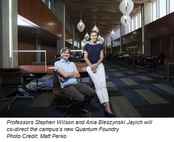
“Under the direction of physics professor Ania Bleszynski Jayich and materials professor Stephen Wilson the foundry will provide a collaborative environment for researchers to continue exploring quantum phenomena, designing quantum materials and building instruments and computers based on the basic principles of quantum mechanics,” Yang added.
Said Joseph Incandela, the campus’s vice chancellor for research, “UC Santa Barbara is a natural choice for the NSF quantum materials Foundry. We have outstanding faculty, researchers, and facilities, and a great tradition of multidisciplinary collaboration. Together with our excellent students and close industry partnerships, they have created a dynamic environment where research gets translated into important technologies.”
“Being selected to build and host the nation’s first Quantum Foundry is tremendously exciting and extremely important,” said Rod Alferness, dean of the College of Engineering. “It recognizes the vision and the decades of work that have made UC Santa Barbara a truly world-leading institution worthy of assuming a leadership role in a mission as important as advancing quantum science and the transformative technologies it promises to enable.”
“Advances in quantum science require a highly integrated interdisciplinary approach, because there are many hard challenges that need to be solved on many fronts,” said Bleszynski Jayich. “One of the big ideas behind the Foundry is to take these early theoretical ideas that are just beginning to be experimentally viable and use quantum mechanics to produce technologies that can outperform classical technologies.”
Doing so, however, will require new materials.
“Quantum technologies are fundamentally materials-limited, and there needs to be some sort of leap or evolution of the types of materials we can harness,” noted Wilson. “The Foundry is where we will try to identify and create those materials.”
Research Areas and Infrastructure
Quantum Foundry research will be pursued in three main areas, or “thrusts”:
- Natively Entangled Materials, which relates to identifying and characterizing materials that intrinsically host anyon excitations and long-range entangled states with topological, or structural, protection against decoherence. These include new intrinsic topological superconductors and quantum spin liquids, as well as materials that enable topological quantum computing.
- Interfaced Topological States, in which researchers will seek to create and control protected quantum states in hybrid materials.
- Coherent Quantum Interfaces, where the focus will be on engineering materials having localized quantum states that can be interfaced with various other quantum degrees of freedom (e.g. photons or phonons) for distributing quantum information while retaining robust coherence.
Developing these new materials and assessing their potential for hosting the needed coherent quantum state requires specialized equipment, much of which does not exist yet. A significant portion of the NSF grant is designated to develop such infrastructure, both to purchase required tools and equipment and to fabricate new tools necessary both to grow and characterize the quantum states in the new materials, Wilson said.
UC Santa Barbara’s deep well of shared materials growth and characterization infrastructure was also a factor in securing the grant. The Foundry will leverage existing facilities, such as the large suite of instrumentation shared via the Materials Research Lab and the California Nanosystems Institute, multiple molecular beam epitaxy (MBE) growth chambers (the university has the largest number of MBE apparatuses in academia), unique optical facilities such as the Terahertz Facility, state-of-the-art clean rooms, and others among the more than 300 shared instruments on campus.
Page 1 of 2
Share on:


Testimonial
"In a year when every marketing dollar mattered, I chose to keep I-Connect007 in our 2025 plan. Their commitment to high-quality, insightful content aligns with Koh Young’s values and helps readers navigate a changing industry. "
Brent Fischthal - Koh YoungSuggested Items
Fresh PCB Concepts: Designing for Success at the Rigid-flex Transition Area
08/28/2025 | Team NCAB -- Column: Fresh PCB ConceptsRigid-flex PCBs come in all shapes and sizes. Manufacturers typically use fire-retardant, grade 4 (FR-4) materials in the rigid section and flexible polyimide materials in the flex region. Because of the small size, some rigid-flex PCBs, like those for hearing aid devices, are among the most challenging to manufacture. However, regardless of its size, we should not neglect the transition area between the rigid and flexible material.
Global Sourcing Spotlight: How to Evaluate Supplier Capabilities Worldwide
08/20/2025 | Bob Duke -- Column: Global Sourcing SpotlightIn global sourcing, the difference between a competitive edge and a catastrophic disruption often comes down to how well you vet your suppliers. Sourcing advanced PCBs, precision components, or materials for complex assemblies demands diligence, skepticism, and more than a little time on airplanes. Here’s how to do your due diligence when evaluating international suppliers and why cutting corners can cost you more than money.
Insulectro and Electroninks Sign North American Distribution Agreement
08/12/2025 | InsulectroElectroninks, a leader in metal organic decomposition (MOD) inks for additive manufacturing and advanced semiconductor packaging, today announced a strategic collaboration and distribution partnership with Insulectro, a premier distributor of materials used in printed electronics and advanced interconnect manufacturing.
Happy’s Tech Talk #41: Sustainability and Circularity for Electronics Manufacturing
08/13/2025 | Happy Holden -- Column: Happy’s Tech TalkI attended INEMI’s June 12 online seminar, “Sustainable Electronics Tech Topic Series: PCBs and Sustainability.” Dr. Maarten Cauwe of imec spoke on “Life Cycle Inventory (LCI) Models for Assessing and Improving the Environmental Impact of PCB Assemblies,” and Jack Herring of Jiva Materials Ltd. spoke on “Transforming Electronics with Recyclable PCB Technology.” This column will review information and provide analysis from both presentations.
Dymax Renews Connecticut Headquarters Lease, Reinforces Long-Term Commitment to Local Community
08/08/2025 | DymaxDymax, a global manufacturer of rapid light-curing materials and equipment, is pleased to announce the renewal and extension of its corporate lease at its 318 Industrial Lane, Torrington, headquarters.