


 The Right Approach: Get Ready for ISO 9001 Version 6
 Dan’s Biz Bookshelf: ‘Still Broke: Walmart’s Remarkable Transformation'
 Driving Innovation: Depth Routing Processes—Achieving Unparalleled Precision in Complex PCBs


Stevens Team Closes in on 'Holy Grail' of Room Temperature Quantum Computing Chips
September 19, 2019 | Stevens Institute of TechnologyEstimated reading time: 3 minutes
To process information, photons must interact. However, these tiny packets of light want nothing to do with each other, each passing by without altering the other. Now, researchers at Stevens Institute of Technology have coaxed photons into interacting with one another with unprecedented efficiency — a key advance toward realizing long-awaited quantum optics technologies for computing, communication and remote sensing.
The team, led by Yuping Huang, an associate professor of physics and director of the Center for Quantum Science and Engineering, brings us closer to that goal with a nano-scale chip that facilitates photon interactions with much higher efficiency than any previous system. The new method, reported as a memorandum in the Sept. 18 issue of Optica, works at very low energy levels, suggesting that it could be optimized to work at the level of individual photons — the holy grail for room-temperature quantum computing and secure quantum communication.
“We’re pushing the boundaries of physics and optical engineering in order to bring quantum and all-optical signal processing closer to reality,” said Huang.
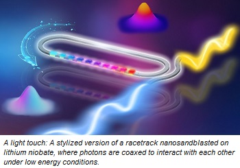
To achieve this advance, Huang’s team fired a laser beam into a racetrack-shaped microcavity carved into a sliver of crystal. As the laser light bounces around the racetrack, its confined photons interact with one another, producing a harmonic resonance that causes some of the circulating light to change wavelength.
That isn’t an entirely new trick, but Huang and colleagues, including graduate student Jiayang Chen and senior research scientist Yong Meng Sua, dramatically boosted its efficiency by using a chip made from lithium niobate on insulator, a material that has a unique way of interacting with light. Unlike silicon, lithium niobate is difficult to chemically etch with common reactive gases. So, the Stevens’ team used an ion-milling tool, essentially a nanosandblaster, to etch a tiny racetrack about one-hundredth the width of a human hair.
Before defining the racetrack structure, the team needed to apply high-voltage electrical pulses to create carefully calibrated areas of alternating polarity, or periodic poling, that tailor the way photons move around the racetrack, increasing their probability of interacting with eachother.
Chen explained that to both etch the racetrack on the chip and tailor the way photons move around it, requires dozens of delicate nanofabrication steps, each requiring nanometer precision. “To the best of our knowledge, we’re among the first groups to master all of these nanofabrication steps to build this system — that’s the reason we could get this result first.”
Moving forward, Huang and his team aim to boost the crystal racetrack’s ability to confine and recirculate light, known as its Q-factor. The team has already identified ways to increase their Q-factor by a factor of at least 10, but each level up makes the system more sensitive to imperceptible temperature fluctuations — a few thousands of a degree — and requires careful fine-tuning.
Still, the Stevens team say they’re closing in on a system capable of generating interactions at the single-photon level reliably, a breakthrough that would allow the creation of many powerful quantum computing components such as photonics logic gates and entanglement sources, which along a circuit, can canvass multiple solutions to the same problem simultaneously, conceivably allowing calculations that could take years to be solved in seconds.
We could still be a while from that point, Chen said, but for quantum scientists the journey will be thrilling. “It’s the holy grail,” said Chen, the paper’s lead author. “And on the way to the holy grail, we’re realizing a lot of physics that nobody’s done before.”
About Stevens Institute of Technology
Stevens Institute of Technology is a premier, private research university situated in Hoboken, New Jersey overlooking the Manhattan skyline. Since our founding in 1870, technological innovation has always been the hallmark and legacy of Stevens’ education and research. Within the university’s three schools and one college, 6,900 undergraduate and graduate students collaborate closely with faculty in an interdisciplinary, student-centric, entrepreneurial environment. Academic and research programs spanning business, computing, engineering, the arts and other fields actively advance the frontiers of science and leverage technology to confront our most pressing global challenges. The university is consistently ranked among the nation’s elite for return on tuition investment, career services and the mid-career salaries of alumni.
Share on:


Testimonial
"The I-Connect007 team is outstanding—kind, responsive, and a true marketing partner. Their design team created fresh, eye-catching ads, and their editorial support polished our content to let our brand shine. Thank you all! "
Sweeney Ng - CEE PCBSuggested Items
EV Group Achieves Breakthrough in Hybrid Bonding Overlay Control for Chiplet Integration
09/12/2025 | EV GroupEV Group (EVG), a leading provider of innovative process solutions and expertise serving leading-edge and future semiconductor designs and chip integration schemes, today unveiled the EVG®40 D2W—the first dedicated die-to-wafer overlay metrology platform to deliver 100 percent die overlay measurement on 300-mm wafers at high precision and speeds needed for production environments. With up to 15X higher throughput than EVG’s industry benchmark EVG®40 NT2 system designed for hybrid wafer bonding metrology, the new EVG40 D2W enables chipmakers to verify die placement accuracy and take rapid corrective action, improving process control and yield in high-volume manufacturing (HVM).
AV Switchblade 600 Loitering Munition System Achieves Pivotal Milestone with First-Ever Air Launch from MQ-9A
09/12/2025 | BUSINESS WIREAeroVironment, Inc. (AV) a global leader in intelligent, multi-domain autonomous systems, announced its Switchblade 600 loitering munition system (LMS) has achieved a significant milestone with its first-ever air launch from an MQ-9A Reaper Unmanned Aircraft System (UAS).
United Electronics Corporation Unveils Revolutionary CIMS Galaxy 30 Automated Optical Inspection System
09/11/2025 | United Electronics CorporationUnited Electronics Corporation (UEC) today announced the launch of its new groundbreaking CIMS Galaxy 30 Automated Optical Inspection (AOI) machine, setting a new industry standard for precision electronics manufacturing quality control. The Galaxy 30, developed and manufactured by CIMS, represents a significant leap forward in inspection technology, delivering exceptional speed improvements and introducing cutting-edge artificial intelligence capabilities.
IPS, SEL Raise the Bar for ENIG Automation in North America
09/11/2025 | Mike Brask, IPSIPS has installed a state-of-the-art automated ENIG plating line at Schweitzer Engineering Laboratories’ PCB facility in Moscow, Idaho. The 81-foot, fully enclosed line sets a new standard for automation, safety, and efficiency in North American PCB manufacturing and represents one of the largest fully enclosed final finish lines in operation.
Smart Automation: Odd-form Assembly—Dedicated Insertion Equipment Matters
09/09/2025 | Josh Casper -- Column: Smart AutomationLarge, irregular, or mechanically unique parts, often referred to as odd-form components, have never truly disappeared from electronics manufacturing. While many in the industry have been pursuing miniaturization, faster placement speeds, and higher-density PCBs, certain market sectors are moving in the opposite direction.