


 The Right Approach: Get Ready for ISO 9001 Version 6
 Dan’s Biz Bookshelf: ‘Still Broke: Walmart’s Remarkable Transformation'
 Driving Innovation: Depth Routing Processes—Achieving Unparalleled Precision in Complex PCBs


New Method for the Measurement of Nano-Structured Light Fields
September 23, 2019 | University of MünsterEstimated reading time: 1 minute
Structured laser light has already opened up various different applications: it allows for precise material machining, trapping, manipulating or defined movement of small particles or cell compartments, as well as increasing the bandwidth for next-generation intelligent computing.
If these light structures are tightly focused by a lens, like a magnifying glass used as burning glass, highly intense three-dimensional light landscapes will be shaped, facilitating a significantly enhanced resolution in named applications. These kinds of light landscapes has paved the way to pioneering applications as Nobel prize awarded STED microscopy.
However, these nano-fields itself could not be measured yet, since components are formed by tight focusing which are invisible for typical measurement techniques. Up to now, this lack of appropriate metrological methods has impeded the breakthrough of nano-structured light landscapes as a tool for material machining, optical tweezers, or high-resolution imaging.
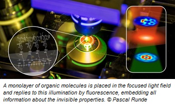
A team around physicist Prof. Dr. Cornelia Denz of the Institute of Applied Physics and chemist Prof. Dr. Bart Jan Ravoo of the Center for Soft Nanoscience (SoN) at the University of Münster successfully developed a nano-tomographic technique which is able to detect the typically invisible properties of nano-structured fields in the focus of a lens – without requiring any complex analysis algorithms or data post-processing. For this purpose, the team combined their knowledge in the field of nano-optics and organic chemistry to realize an approach based on a monolayer of organic molecules. This monolayer is placed in the focused light field and replies to this illumination by fluorescence, embedding all information about the invisible properties.
By the detection of this reply the distinct identification of the nano-field by a single, fast and straightforward camera image is enabled. “This approach finally opens the till now unexploited potential of these nano-structured light landscapes for many more applications,” says Cornelia Denz, who is heading the study. The study has been published in the journal “Nature Communications”.
Share on:


Testimonial
"In a year when every marketing dollar mattered, I chose to keep I-Connect007 in our 2025 plan. Their commitment to high-quality, insightful content aligns with Koh Young’s values and helps readers navigate a changing industry. "
Brent Fischthal - Koh YoungSuggested Items
MEMS & Imaging Sensors Summit to Spotlight Sensing Revolution for Europe’s Leadership
09/11/2025 | SEMIIndustry experts will gather November 19-20 at the SEMI MEMS & Imaging Sensors Summit 2025 to explore the latest breakthroughs in AI-driven MEMS and imaging optimization, AR/VR technologies, and advanced sensor solutions for critical defence applications.
Direct Imaging System Market Size to Hit $4.30B by 2032, Driven by Increasing Demand for High-Precision PCB Manufacturing
09/11/2025 | Globe NewswireAccording to the SNS Insider, “The Direct Imaging System Market size was valued at $2.21 Billion in 2024 and is projected to reach $4.30 Billion by 2032, growing at a CAGR of 8.68% during 2025-2032.”
I-Connect007’s Editor’s Choice: Five Must-Reads for the Week
07/04/2025 | Marcy LaRont, I-Connect007For our industry, we have seen several bullish market announcements over the past few weeks, including one this week by IDC on the massive growth in the global server market. We’re also closely watching global trade and nearshoring. One good example of successful nearshoring is Rehm Thermal Systems, which celebrates its 10th anniversary in Mexico and the official opening of its new building in Guadalajara.
Driving Innovation: Direct Imaging vs. Conventional Exposure
07/01/2025 | Simon Khesin -- Column: Driving InnovationMy first camera used Kodak film. I even experimented with developing photos in the bathroom, though I usually dropped the film off at a Kodak center and received the prints two weeks later, only to discover that some images were out of focus or poorly framed. Today, every smartphone contains a high-quality camera capable of producing stunning images instantly.
United Electronics Corporation Advances Manufacturing Capabilities with Schmoll MDI-ST Imaging Equipment
06/24/2025 | United Electronics CorporationUnited Electronics Corporation has successfully installed the advanced Schmoll MDI-ST (XL) imaging equipment at their advanced printed circuit board facility. This significant technology investment represents a continued commitment to delivering superior products and maintaining their position as an industry leader in precision PCB manufacturing.