


 Driving Innovation: Mechanical and Optical Processes During Rigid-flex Production
 It’s Only Common Sense: Your Biggest Competitor Is Complacency
 The Chemical Connection: Onshoring PCB Production—Daunting but Certainly Possible


Ultra-Sensitive Sensors from Impure Diamonds
September 30, 2019 | Kyoto UniversityEstimated reading time: 1 minute
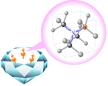
A Kyoto University research group has developed the longest spin coherence times at room temperature of an NV centre in diamond, using an artificially synthesised phosphorus-doped n-type diamond.
Furthermore, they succeeded in recording the highest magnetic field sensitivity of a single NV quantum sensor. Their findings were reported in Nature Communications.
An NV centre in diamond emerges when a carbon atom in the lattice is replaced by a nitrogen atom, and one of its adjacent atoms is removed. This generates a 'hole' in the lattice, known as a 'vacancy', hence the name N (nitrogen) V (Vacancy) centre. This vacancy attracts an electron and takes the property of a magnet.
Owing to its stability and sensitivity, NV centres in diamond are a major focus for researchers who hope to apply the technology to develop ultrasensitive quantum sensors, with applications even for devices in the life sciences.
The diamond samples used in NV-centric research have been mainly pure diamonds due to the conventional wisdom that impurities would hold electron spins that generate noise. However, the research team, collaborating with the National Institute of Advanced Industrial Science and Technology, found that phosphorus-doped n-type diamonds have remarkably long spin-coherence times.
After careful study, the team found that the diamonds have the longest inhomogeneous spin-dephasing time and spin decoherence time recorded in room-temperature solid-state systems and the highest magnetic field sensitivity.
Norikazu Mizuochi from Kyoto University's Institute for Chemical Research, who lead the study, explains that the team was surprised that adding impurities to the NV diamond was the key to improve its spin coherence.
"Phosphorus is one of the causes of magnetic noise due to its electron spin," explains Mizuochi. "We hope our new results will greatly contribute to the ever-expanding field of quantum technology."
Share on:


Testimonial
"Your magazines are a great platform for people to exchange knowledge. Thank you for the work that you do."
Simon Khesin - Schmoll MaschinenSuggested Items
HPE Now Powers New AI-Ready Supercomputer Set to Transform Environmental Forecasting in New Zealand
09/22/2025 | BUSINESS WIREHPE announced that Earth Sciences New Zealand (formally NIWA) of Aotearoa (New Zealand) selected HPE Cray XD2000, purpose-built for AI and simulation workloads, to accelerate the organization’s environmental science and precision of meteorological forecasting.
PC Graphics Add-in Board Shipments Up 27% QoQ in 2Q25
09/03/2025 | Jon Peddie ResearchAccording to a new research report from the analyst firm Jon Peddie Research, the growth of the global PC-based graphics add-in board market reached 11.6 million units in Q2'25 and desktop PC CPUs shipments increased to 21.7 million units.
PC GPU Shipments Up 8.4% in 2Q25 on Pre-Tariff Demand
09/02/2025 | Jon Peddie ResearchJon Peddie Research reports the growth of the global PC-based graphics processor unit (GPU) market reached 74.7 million units in Q2'25, and PC CPU shipments increased to 66.9 million units.
20 Years of Center Nanoelectronic Technologies (CNT) – Backbone of German Semiconductor Research Celebrates Anniversary
08/14/2025 | Fraunhofer IPMSThe Center Nanoelectronic Technologies (CNT) of the Fraunhofer Institute for Photonic Microsystems (IPMS) is celebrating its 20th anniversary this year. Since its founding in 2005, it has developed into a pillar of applied semiconductor research in Germany and Europe. With its unique research cleanroom and equipment adhering to the 300-mm wafer industry standard, CNT is unparalleled in Germany and serves as a central innovation driver for the microelectronics industry.
Q2 Client CPU Shipments Increased 8% from Last Quarter, Up 13% YoY
08/13/2025 | Jon Peddie ResearchJon Peddie Research reports that the global client CPU market expanded for two quarters in a row, and in Q2’25, it showed unseasonal growth of 7.9% from last quarter, while server CPU shipments increased 22% year over year.