


 It’s Only Common Sense: Hire for Hunger, Train for Skill
 Dan’s Biz Bookshelf: ‘The 'NVIDIA Way: Jensen Huang and the Making of a Tech Giant’


Silicon Technology Boost with Graphene and 2D Materials
October 1, 2019 | ICFOEstimated reading time: 2 minutes
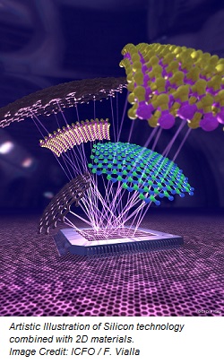
Silicon semiconductor technology has done marvels for the advancement of our society, who has benefited tremendously from its versatile use and amazing capabilities. The development of electronics, automation, computers, digital cameras and recent smartphones based on this material and its underpinning technology has reached skyrocket limits, downscaling the physical size of devices and wires to the nanometre regime.
Although this technology has been developing since the late 1960s, the miniaturization of circuits seems to have reached a possible halt, since transistors can only be shrunk down to a certain size and not further beyond. Thus, there is a pressing need to complement Si CMOS technology with new materials, and fulfil the future computing requirements as well as the needs for diversification of applications.
Now, graphene and related two-dimensional (2D) materials offer prospects of unprecedented advances in device performance at the atomic limit. Their amazing potential has proven to be a possible solution to overcome the limitations of silicon technology, where the combination of 2D materials with silicon chips promises to surpass the current technological limitations.
In the new review article in Nature, a team of international researchers including ICFO researchers Dr. Stijn Goossens and ICREA Prof at ICFO Frank Koppens, and industrial leaders from IMEC and TSMC have come together to provide an in-depth and thorough review about the opportunities, progress and challenges of integrating atomically thin materials with Si-based technology. They give insights on how and why 2D materials (2DMs) could overcome current challenges posed by the existing technology and how they can enhance both device component function and performance, to boost the features of future technologies, in the areas of computational and non-computational applications.
For non-computational applications, they review the possible integration of these materials for future cameras, low power optical data communications and gas and bio-sensors. In particular, image sensors and photodetectors, where graphene and 2DMs could enable a new vision in the infrared and terahertz range in addition to the visible range of the spectrum. These can serve for example in autonomous vehicle, security at airports and augmented reality.
For computational systems, and in particular in the field of transistors, they show how challenges such as doping, contact resistance and dielectrics/encapsulation can be diminished when integrating 2DMs with Si technology. 2DMs could also radically improve memory and data storage devices with novel switching mechanisms for meta-insulator-metal structures, avoid sneak currents in memory arrays, or even push performance gains of copper wired based circuitry by adhering graphene to the ultrathin copper barrier materials and thus reduce resistance, scattering and self-heating.
The review provides insight to all stakeholders about the challenges and impact of solving the 2D material integration with CMOS technology. It provides a roadmap of 2D integration and CMOS technology, pinpointing the stage at which all challenges regarding growth, transfer, interface, doping, contacting, and design are currently standing today and what possible processes are expected to be resolved to achieve such goals of moving from a research laboratory environment to a pilot line for production of the first devices that combine both technologies.
The first 2D material-CMOS roadmap, as presented in this review, gives an exciting glimpse in the future, with first pilot production to be expected already in just a few years from now.
Share on:


Testimonial
"Our marketing partnership with I-Connect007 is already delivering. Just a day after our press release went live, we received a direct inquiry about our updated products!"
Rachael Temple - AlltematedSuggested Items
Nortech Systems Launches Power over Fiber Technology Platform for EMI-Sensitive Applications
04/08/2026 | Globe NewswireNortech Systems Incorporated, a leading provider of design and manufacturing solutions for complex electromedical devices and electromechanical systems, has announced the launch of its Power over Fiber technology platform.
Flexible Thinking: Designing Flex Circuits for Dynamic Reliability
04/09/2026 | Joe Fjelstad -- Column: Flexible ThinkingFlex circuits flex. No surprises there. However, they are also very commonly designed into products because they are thin and offer consistent thickness and dielectric properties, attributes highly prized by present-day product designers of personal electronics. This would include smartphones and, increasingly, wearable electronics for medical monitoring and even fashion.
Understanding Tolerances in Flexible Circuit Design
04/01/2026 | Chris Clark, Flexible Circuit TechnologiesThe challenge with cumulative tolerances is meeting the dimensional requirements for items dimensioned on a drawing or specification for a flexible or rigid-flex circuit. It is critical to understand the fabrication processes and how features are defined when creating your tolerance requirements.
Target Condition: An Exploration of Flooding PCB Layers
04/02/2026 | Kelly Dack -- Column: Target ConditionThe concept of flooding PCB layers with copper has been around for so long, you’d think we’d have it mastered. We haven’t. (Oh, and by “we,” I mean design engineers and the software tools we depend on.) Years ago, PCB artwork was created by hand using light tables, with tape applied to Mylar. Signals were slow, traces were relatively wide, and high-current paths were simply “beefed up” with wider copper. Signal integrity wasn’t yet a driving concern. Today, solid return paths are fundamental to robust design. We understand the importance of continuous reference planes for signal integrity and EMI control.
New, Greener Solutions for Etch: Novel Copper Extraction
03/30/2026 | Richard Nichols, GreenSource Engineering“Novel” is a typical marketing phrase that implies new and unique, but often “novel” actually means an established technology being applied to a new field or application. This, in turn, is often driven by newly relevant external motivation. GreenSource has been working on just such a solution: novel copper extraction, offering a better and greener alternative to traditional LLE control systems for cupric chloride etch.