


 It’s Only Common Sense: Hire for Hunger, Train for Skill
 Dan’s Biz Bookshelf: ‘The 'NVIDIA Way: Jensen Huang and the Making of a Tech Giant’


Energy Efficient Power Electronics—Gallium Oxide Power Transistors with Record Levels
October 2, 2019 | FBHEstimated reading time: 1 minute
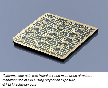
With as little space as possible, they should be able to achieve ever higher power densities with low energy consumption and thus work more efficiently. Conventional components reach their limits here. As a result, scientists around the world are researching novel materials and components that meet these requirements. The Ferdinand Braun Institute, Leibniz Institute for High Frequency Technology (FBH) has now achieved a breakthrough with transistors based on gallium oxide (ß-Ga2O3).
The newly developed ß-Ga2O3 MOSFETs (dt. Metal-oxide-semiconductor field effect transistor) provide a high breakdown voltage with high current conductivity. With 1.8 kilovolts of breakdown voltage and a record output of 155 megawatts per square centimeter, they achieve unique global metrics close to the theoretical material limit of gallium oxide. At the same time, the breakthrough field strengths achieved are far greater than those of established large band gap semiconductors such as silicon carbide or gallium nitride.
Optimized layer structure and gate topology
To achieve these improvements, the FBH team started on the layer structure and the gate topology. The basis was provided by substrates from the Leibniz Institute for Crystal Growth (IKZ) with an optimized epitaxial layer structure. This reduced the defect density and improved the electrical properties. This leads to lower resistances when switched on. The gate is the central "switching point" in field effect transistors, which is controlled by the gate-source voltage. Its topology has been further developed so that the high field strengths at the gate edge could be reduced. This in turn leads to higher breakdown voltages.
Share on:


Testimonial
"Our marketing partnership with I-Connect007 is already delivering. Just a day after our press release went live, we received a direct inquiry about our updated products!"
Rachael Temple - AlltematedSuggested Items
Target Condition: An Exploration of Flooding PCB Layers
04/02/2026 | Kelly Dack -- Column: Target ConditionThe concept of flooding PCB layers with copper has been around for so long, you’d think we’d have it mastered. We haven’t. (Oh, and by “we,” I mean design engineers and the software tools we depend on.) Years ago, PCB artwork was created by hand using light tables, with tape applied to Mylar. Signals were slow, traces were relatively wide, and high-current paths were simply “beefed up” with wider copper. Signal integrity wasn’t yet a driving concern. Today, solid return paths are fundamental to robust design. We understand the importance of continuous reference planes for signal integrity and EMI control.
Happy’s Tech Talk #47: Automation for Complex Multilayer Fabrication Stackups
03/31/2026 | Happy Holden -- Column: Happy’s Tech TalkMultilayer stackups have evolved dramatically as they’ve been adopted for high-performance computing (HPC) and artificial intelligence (AI) server applications. These high-speed, high I/O designs require the designer and fabricator to manage more boundary conditions than ever before. In practice, the stackup is no longer “just a stackup.” It becomes the foundation for signal integrity, reliability, manufacturability, and cost.
SCHMID Group Wins Major Order for Wet-Process Equipment for AI & HPC Infrastructure
03/11/2026 | SCHMID GroupSCHMID Group, a leading global supplier of advanced wet process equipment for the electronics manufacturing industry, has secured a lower two-digit million-USD purchase order from a major Asian high-end PCB manufacturer for a new HDI multilayer production line.
Standard of Excellence: Building the Board of the Future—Materials, Methods, and Mindset
02/18/2026 | Anaya Vardya -- Column: Standard of ExcellenceThe future of PCB manufacturing is here. The products we’re being asked to build today would have been called “advanced” just a few years ago. What was once special is now standard, and what was once impossible is now expected. The challenge and the opportunity lie in leading the charge to the next frontier of printed circuit board design, materials, and manufacturing discipline. To build the board of the future, we need new materials, smarter methods, and a mindset of innovation anchored in flawless execution.
UHDI Fundamentals: An Overview of UHDI Layer Types
01/02/2026 | Anaya Vardya, American Standard CircuitsUHDI layer types include core, sequential lamination build-up; microvia; embedded and passive antennas and inductors; and embedded functional, protective, and hybrid rigid-flex layers. Together, they enable ultra-fine features, dense interconnects, high-frequency performance, and miniaturized system designs. UHDI typically requires multiple SBU cycles, where thin dielectric and copper layers are drilled for microvias, plated, imaged, and laminated sequentially to build up to the final design from the inside out.