


 It’s Only Common Sense: Hire for Hunger, Train for Skill
 Dan’s Biz Bookshelf: ‘The 'NVIDIA Way: Jensen Huang and the Making of a Tech Giant’


Taking 2D Materials to the MAX
October 17, 2019 | KAUSTEstimated reading time: 3 minutes
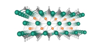
A class of atomically thin 2D compounds, known as MXenes, have a unique combination of properties that are useful for electronic and sensing applications.
Discovered by researchers at Drexel University as electrodes for energy applications, MXenes have become a research focus for KAUST. Husam Alshareef and his team specialize in creating nanomaterials for electronic and energy applications. They turn them into devices, such as supercapacitors, batteries and sensors. The chemically active surface and highly conducting core of MXenes make them an ideal candidate material for the group’s cutting-edge materials research.
MXene membranes, like these fabricated in Alshareef's lab, are used for energy storage, sensing and osmotic power generation.
MXenes typically consist of a core of titanium and carbon atoms, just a few atoms thick. This metallic material (a carbide or nitride) has electrical conductivity comparable to a copper wire. The upper and lower surface of the MXene is covered with metal-oxygen (e.g. Ti-O) and metal-hydroxyl (e.g. Ti-OH) bonds, which are chemically and electrochemically active. “This combination of properties makes MXenes unique,” Alshareef explains.
“Researchers at KAUST have made groundbreaking contributions to applications of MXenes in electronic devices and sensors,” says Yury Gogotsi, a professor from Drexel University in the United States, one of the discoverers of MXenes. “They have moved them from the material stage to the device stage thanks to their experience with electronics. This is very important and may be a defining moment in the practical implementation of MXenes in industry.”
MXenes can be used to create better sensors, touch screens, photodetectors and composites.
Page 1 of 2
Share on:


Testimonial
"Advertising in PCB007 Magazine has been a great way to showcase our bare board testers to the right audience. The I-Connect007 team makes the process smooth and professional. We’re proud to be featured in such a trusted publication."
Klaus Koziol - atgSuggested Items
Nortech Systems Launches Power over Fiber Technology Platform for EMI-Sensitive Applications
04/08/2026 | Globe NewswireNortech Systems Incorporated, a leading provider of design and manufacturing solutions for complex electromedical devices and electromechanical systems, has announced the launch of its Power over Fiber technology platform.
Flexible Thinking: Designing Flex Circuits for Dynamic Reliability
04/09/2026 | Joe Fjelstad -- Column: Flexible ThinkingFlex circuits flex. No surprises there. However, they are also very commonly designed into products because they are thin and offer consistent thickness and dielectric properties, attributes highly prized by present-day product designers of personal electronics. This would include smartphones and, increasingly, wearable electronics for medical monitoring and even fashion.
Understanding Tolerances in Flexible Circuit Design
04/01/2026 | Chris Clark, Flexible Circuit TechnologiesThe challenge with cumulative tolerances is meeting the dimensional requirements for items dimensioned on a drawing or specification for a flexible or rigid-flex circuit. It is critical to understand the fabrication processes and how features are defined when creating your tolerance requirements.
Target Condition: An Exploration of Flooding PCB Layers
04/02/2026 | Kelly Dack -- Column: Target ConditionThe concept of flooding PCB layers with copper has been around for so long, you’d think we’d have it mastered. We haven’t. (Oh, and by “we,” I mean design engineers and the software tools we depend on.) Years ago, PCB artwork was created by hand using light tables, with tape applied to Mylar. Signals were slow, traces were relatively wide, and high-current paths were simply “beefed up” with wider copper. Signal integrity wasn’t yet a driving concern. Today, solid return paths are fundamental to robust design. We understand the importance of continuous reference planes for signal integrity and EMI control.
New, Greener Solutions for Etch: Novel Copper Extraction
03/30/2026 | Richard Nichols, GreenSource Engineering“Novel” is a typical marketing phrase that implies new and unique, but often “novel” actually means an established technology being applied to a new field or application. This, in turn, is often driven by newly relevant external motivation. GreenSource has been working on just such a solution: novel copper extraction, offering a better and greener alternative to traditional LLE control systems for cupric chloride etch.