


 Beyond the Board: Early Engagement Means Faster Prototyping for Defense Programs
 Defense Speak Interpreted: The Autonomous Plane Battle—Skyborg Vs. Loyal Wingman
 American Made Advocacy: Congress Back from Break With Work To Do


New Type of Transistor One Step Closer
October 18, 2019 | University of GroningenEstimated reading time: 2 minutes
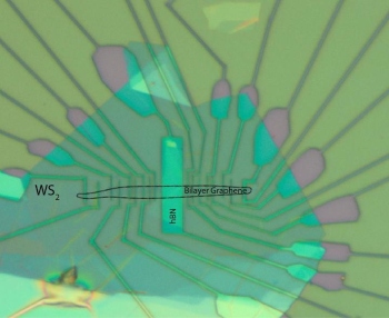
In order to make transistors that operate using the spin of electrons, rather than their charge, it is necessary to find a way of switching spin currents on and off. Furthermore, the lifetime of the spins should at least be equal to the time taken for these electrons to travel through a circuit. University of Groningen scientists have now taken an important step forward by creating a device that meets both of these requirements, based on a double layer of graphene on top of a layer of tungsten disulfide. Their results have been published on 16 October in the journal Physical Review B.
Graphene, a two-dimensional form of carbon, is an excellent conductor of electron spins. However, it is difficult to manipulate spin currents in this material. Spin is a quantum mechanical property of electrons, which makes them behave like tiny magnets. The Physics of Nanodevices group at the University of Groningen, led by Professor Bart van Wees, is working on this problem. They have previously shown that it is possible to control spin currents if the graphene is placed on top of a layer of tungsten disulphide (another 2D material).
New Technique
"However, this approach reduces the lifetime of the spins," explains Siddhartha Omar, a postdoc in the Van Wees group. Tungsten is a metal, and its atoms influence the electrons passing through the graphene, dissipating the spin currents. This led Omar to use a double layer of graphene on the tungsten disulphide, based on the theory that electrons passing through the upper layer should 'feel' less of the metal atoms' influence.
Omar also used another new technique, in which two different types of spin current are passed through the graphene. Spin is a magnetic moment that has a given direction. In normal materials, the spins are not aligned. However, the magnetic moment of spin currents—like that of magnets—has a preferential alignment. Relative to the material through which the electrons are passing, their spins can either have an in-plane orientation or an out-of-plane orientation.
Energy Level
"We found that, as the electrons pass through the outer graphene layer, the in-plane spins are dissipated very quickly—in mere picoseconds. However, the lifetime of the out-of-plane spins is about one hundred times longer." This means that, even in the presence of tungsten disulphide, one component of spin currents (spins with an out-of-plane orientation) can travel far enough to be used in devices such as transistors.
The energy level of the spin currents observed by Omar caused them to pass through the upper layer of graphene. This energy level can be boosted by applying an electric field, pushing the spin currents into the lower layer. "Down there, the spins will feel the full effect of the metal atoms and the spin currents will quickly dissipate," Omar explains. This ability to switch the spin current off using an electric field is important, as it could be used to 'gate' transistors based on this technology.
"Unfortunately, certain technical limitations of the substrate on which we built these devices prevent us from creating electric fields that are strong enough to produce this gating effect," says Omar. "However, we have shown that it is possible to send spin currents through a heterostructure made of graphene and tungsten disulphide. That is an important step towards the creation of a spin transistor."
Share on:


Testimonial
"Advertising in PCB007 Magazine has been a great way to showcase our bare board testers to the right audience. The I-Connect007 team makes the process smooth and professional. We’re proud to be featured in such a trusted publication."
Klaus Koziol - atgSuggested Items
The Marketing Minute: Marketing With Layers
10/15/2025 | Brittany Martin -- Column: The Marketing MinuteMarketing to a technical audience is like crafting a multilayer board: Each layer serves a purpose, from the surface story to the buried detail that keeps everything connected. At I-Connect007, we’ve learned that the best marketing campaigns aren’t built linearly; they’re layered. A campaign might start with a highly technical resource, such as an in-depth article, a white paper, or a podcast featuring an engineer delving into the details of a process. That’s the foundation, the substance that earns credibility.
EDADOC Ushers in a New Era of Robotics Innovation
10/07/2025 | Edy Yu, Editor-in-Chief, ECIOOn Sept. 11, Shanghai Zhiyuan Technology Co., Ltd. (MScape) made a stunning debut at Shanghai’s 2025 Fourth North Bund Cybersecurity Forum and Cyber Intelligence Security Frontier Technology and Equipment Exhibition. The company presented the world’s first Dvorak super heterogeneous architecture and the Zhijing T-series-embodied intelligence (robotics) edge computing power platform. This has been a game-changer in the cybersecurity technology field, filling the gap in the domestic robotics core computing power platform.
Connect the Dots: Evolution of PCB Manufacturing—Lamination
10/02/2025 | Matt Stevenson -- Column: Connect the DotsWhen I wrote The Printed Circuit Designer's Guide to...™ Designing for Reality, it was not a one-and-done effort. Technology is advancing rapidly. Designing for the reality of PCB manufacturing will continue to evolve. That’s why I encourage designers to stay on top of the tools and processes used during production, to ensure their designs capitalize on the capabilities of their manufacturing partner.
Driving Innovation: Mastering Panel Warpage
09/23/2025 | Simon Khesin -- Column: Driving InnovationDuring the complex and multi-step process of PCB fabrication, a panel's flatness is constantly at risk. A host of factors can introduce warpage, bending, and unevenness, presenting a fundamental challenge to achieving high-precision results. This deformation (sometimes referred to as “bow and twist”), even on a microscopic scale, can lead to critical defects during subsequent stages, such as component surface mounting (e.g., tombstoning, solder opens) and the PCB's long-term functional reliability.
Beyond Design: Slaying Signal Integrity Villains
09/17/2025 | Barry Olney -- Column: Beyond DesignHigh-speed PCB design is a balancing act, where subtle oversights can develop into major signal integrity nightmares. Some culprits lie dormant during early validation, only to reveal themselves later through workflow disruptions and elusive performance bottlenecks. Take crosstalk, for example. What begins as a stray signal coupling between traces can ripple through the design, ultimately destabilizing the power distribution network. Each of these troublemakers operates with signature tactics, but they also have well-known vulnerabilities.