


 Powering the Future: When Material Choice Defines RF Performance
 Learning with Leo: The Cost of Cleaning and Protecting the Ozone Layer
 Nolan’s Notes: Cleaning With Smaller Geometries


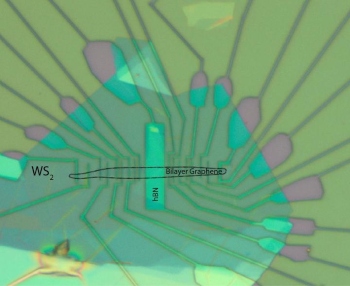
In order to make transistors that operate using the spin of electrons, rather than their charge, it is necessary to find a way of switching spin currents on and off. Furthermore, the lifetime of the spins should at least be equal to the time taken for these electrons to travel through a circuit. University of Groningen scientists have now taken an important step forward by creating a device that meets both of these requirements, based on a double layer of graphene on top of a layer of tungsten disulfide. Their results have been published on 16 October in the journal Physical Review B.
Graphene, a two-dimensional form of carbon, is an excellent conductor of electron spins. However, it is difficult to manipulate spin currents in this material. Spin is a quantum mechanical property of electrons, which makes them behave like tiny magnets. The Physics of Nanodevices group at the University of Groningen, led by Professor Bart van Wees, is working on this problem. They have previously shown that it is possible to control spin currents if the graphene is placed on top of a layer of tungsten disulphide (another 2D material).
New Technique
"However, this approach reduces the lifetime of the spins," explains Siddhartha Omar, a postdoc in the Van Wees group. Tungsten is a metal, and its atoms influence the electrons passing through the graphene, dissipating the spin currents. This led Omar to use a double layer of graphene on the tungsten disulphide, based on the theory that electrons passing through the upper layer should 'feel' less of the metal atoms' influence.
Omar also used another new technique, in which two different types of spin current are passed through the graphene. Spin is a magnetic moment that has a given direction. In normal materials, the spins are not aligned. However, the magnetic moment of spin currents—like that of magnets—has a preferential alignment. Relative to the material through which the electrons are passing, their spins can either have an in-plane orientation or an out-of-plane orientation.
Energy Level
"We found that, as the electrons pass through the outer graphene layer, the in-plane spins are dissipated very quickly—in mere picoseconds. However, the lifetime of the out-of-plane spins is about one hundred times longer." This means that, even in the presence of tungsten disulphide, one component of spin currents (spins with an out-of-plane orientation) can travel far enough to be used in devices such as transistors.
The energy level of the spin currents observed by Omar caused them to pass through the upper layer of graphene. This energy level can be boosted by applying an electric field, pushing the spin currents into the lower layer. "Down there, the spins will feel the full effect of the metal atoms and the spin currents will quickly dissipate," Omar explains. This ability to switch the spin current off using an electric field is important, as it could be used to 'gate' transistors based on this technology.
"Unfortunately, certain technical limitations of the substrate on which we built these devices prevent us from creating electric fields that are strong enough to produce this gating effect," says Omar. "However, we have shown that it is possible to send spin currents through a heterostructure made of graphene and tungsten disulphide. That is an important step towards the creation of a spin transistor."


