


 The Marketing Minute: If Your Marketing Budget Gets Cut in Half, Then What?
 Punching Out: How Are the Big Boys in Electronics Doing?
 It’s Only Common Sense: Complexity Is the Enemy of Profit


Aismalibar North America to Exhibit at Strategies in Light
January 27, 2020 | AismalibarEstimated reading time: 2 minutes
AISMALIBAR is happy to exhibit at this year’s Strategies in Light trade show in San Diego, CA on February 11−13, 2020. Strategies in Light is the leading LED and lighting event in North America and has been for more than 15 years. Aismalibar North America encourages visitors to come and view cutting-edge thermal management solutions.
Strategies in light covers every aspect of lighting to provide a 360-degree view of the market and offers a platform where professionals can learn, collaborate, and connect face-to-face. More than 200 exhibitors will showcase the latest products, technologies and services.
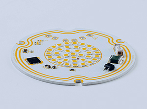
Aismalibar will showcase their newest technology, COBRITHERM ULTRATHIN 4W – TG180ºC−150ºC MOT. An Insulated Metal Substrate (IMS) based on an aluminum cladding with an ED copper sheet on the opposite side, it contains an innovative 35mm ultra-thin polymer-ceramic dielectric layer of its own formulation, offering industry-leading thermal conductivity and high dielectric strength. It also offers strong MOT, High Tg and Low CTE values, which are the key elements for performance of the MPCB operating at high temperatures.
In addition, Aismalibar will feature THIN LAM HTC 3,2W - Tg180°C - Td 420°C - Low CTE. By THIN LAM allows for easy temperature reduction of your board allowing for an increase the power or the processor clock speed to obtain better performance on the same electronic design. FR4 PCBs with high density of thermal vias can be replaced by a standard double side PCBs constructed with THIN LAM without the needs of thermal vias.
Finally, Aismalibar will showcase the BOND SHEET PRE PREG 3,2W - Tg180ºC - Low CTE. Aismalibar’s high thermal BOND SHEET (Thermal Pre Preg) can be used for different applications on multilayer PCB and MPCB industry. By using BOND SHEET, dielectric layers become thermally conductive and are ideal to release heat from the electronic components located on the functional copper sideways and to the heatsink.
About AISMALIBAR
Founded in 1934 and based in Barcelona, Spain, Aismalibar manufactures high end Copper and Metal Clad Laminates for the Printed Circuit Board Industry. Aismalibar’s expertise lies in offering the best solutions to reduce the operational temperature of the Printed Circuit Boards. Aismalibar materials ensure quality and reliability of all the products that incorporate them.
Aismalibar has implemented a 100% proof test with 1-3KV (High Pot Test) to every IMS laminate that is produced. These materials minimize the use of supplementary fans or heat sinks, thus reducing production costs. Aismalibar now operates globally through several subsidiaries. Our priorities are, and have always been technological innovation and customer satisfaction.
Share on:


Testimonial
"In a year when every marketing dollar mattered, I chose to keep I-Connect007 in our 2025 plan. Their commitment to high-quality, insightful content aligns with Koh Young’s values and helps readers navigate a changing industry. "
Brent Fischthal - Koh YoungSuggested Items
I-Connect007 Releases The Printed Circuit Designer’s Guide to… Direct Metallization: A Guide to Complex PCB Fabrication
05/13/2026 | I-Connect007As PCB complexity continues to accelerate, fabricators and OEMs are reevaluating long-standing manufacturing processes to meet the demands of AI, HDI, advanced packaging, and next-generation electronics. To address these evolving challenges, I-Connect007 is proud to announce the release of The Printed Circuit Designer’s Guide to… Direct Metallization: A Guide to Complex PCB Fabrication, authored by MacDermid Alpha Solution’s Carmichael Gugliotti.
Driving Innovation: Selecting the Right Laser Source
04/28/2026 | Simon Khesin -- Column: Driving InnovationWhen I first joined Schmoll Maschinen, I brought experience from almost every PCB process, except for laser. As I immersed myself in laser processing, I realized why it can seem so daunting to a newcomer. The complexity arises from three intersecting factors: A vast variety of laser sources: CO2, UV-nano, green-pico, UV-pico, IR-pico, and others; a diverse range of applications: Drilling, cutting, ablation, and more; and an extensive list of materials: These have vastly different absorption rates. Choosing the right machine or laser source is rarely trivial. Even for experienced engineers, answering "Which source is best?" requires examining the business's specific goals.
Institute of Circuit Technology Spring Seminar 2026: A Bright Future in Europe
04/23/2026 | Pete Starkey, I-Connect007Through the leafy lanes and spring flowers of Warwickshire and back to Meridan, the traditional centre of England, and now officially part of the Metropolitan Borough of Solihull in the county of the West Midlands, I attended the Annual General Meeting and Spring Seminar of the Institute of Circuit Technology (ICT) on April 14. Out of the AGM came notable changes in leadership at the top of the Institute: the retirement of Mat Beadel as chair and Emma Hudson as technical director. Effective May 1, Steve Driver is the new chair, and Alun Morgan is the new technical director.
ACCM Unveils Negative and Near-zero CTE Materials for Large-Format AI Chips
04/21/2026 | Advanced Chip and Circuit MaterialsAdvanced Chip and Circuit Materials, Inc. (ACCM) has launched two new materials: Celeritas HM50, with a negative coefficient of thermal expansion (CTE) of -8 ppm/°C to offset the positive CTE and expansion of copper with temperature on circuit boards, and Celeritas HM001, with near-zero CTE and the low-loss performance needed for high-speed signal layers to 224 Gb/s and faster in artificial intelligence (AI) circuits.
Fresh PCB Concepts: Designing PCBs for Harsh Environments—Reliability Is Engineered Upstream
04/23/2026 | Team NCAB -- Column: Fresh PCB ConceptsWhen engineers hear the phrase “harsh environment,” they usually think of the extreme temperature swings, vibration and shock, pressure changes, or radiation in aerospace. However, aerospace is not the only harsh environment where electronic assemblies must survive. Automotive power electronics, downhole oil and gas tools, marine controls, rail systems, defense platforms, and industrial automation equipment all expose PCBs to environments that are equally unforgiving. The stress mechanisms may differ, but the physics does not.