


 The Hidden Enabler of Autonomous Warfare: Advanced PCB Technologies Behind Defense AI
 It’s Only Common Sense: Stay Curious, My Friends


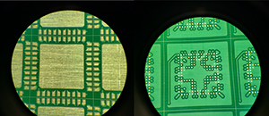
Quik-Pak, a provider of innovative microelectronic packaging and assembly solutions, today announced its substrate design, fabrication and assembly service. Utilizing virtually any substrate type, Quik-Pak can create turnkey solutions for substrate-based assemblies to accommodate customers’ unique packaging requirements, with delivery times at least 50% faster than those of competitive services.
Quik-Pak’s substrate service targets both ICs and MEMS, and its ability to accommodate all types of substrates provides engineering flexibility that allows greater design freedom for a wide range of advanced packages. Quik-Pak has offered this capability, in a limited fashion, for several years. Its success has spurred the company to step up activity—particularly in the face of broadening demand for custom packaging solutions that can fill the gaps not met by standard, off-the-shelf packages.
One key driver for this demand is the increased need for custom RF packages in the face of 5G’s imminent rollout. Technologies in which Quik-Pak specializes, such as laminate quad flat no-lead (QFN) and organic QFN for flip-chips, are well suited to integration and customization. The service can also accommodate 3D packaging, ball grid arrays (BGAs), systems-in-package (SiPs) and multichip modules (MCMs).
According to Quik-Pak Chief Operating Officer Ken Molitor, “We can tune our process to optimize the customer’s desired parameter—size, performance, application—creating a solution in about five weeks, from initial consultation to finished assembly. Other services can take five weeks to complete the design alone and up to 16 weeks to deliver the assembled package. With this combination of quality and speed, Quik-Pak is poised to broaden the reach of our service to address new markets and applications, such as military, medical, sensors and other custom arenas.”
Quik-Pak will be showcasing its full range of capabilities, including its new substrate service offering, in the expo hall at the 16th annual IMAPS International Conference on Device Packaging. The company is also a sponsor of the event, to be held March 2-5, 2020, in Fountain Hills, Ariz.


