


 The Hidden Enabler of Autonomous Warfare: Advanced PCB Technologies Behind Defense AI
 It’s Only Common Sense: Stay Curious, My Friends


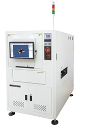
Test Research, Inc. (TRI), the leading test and inspection systems provider for the electronics manufacturing industry, is pleased to announce the release of the high-resolution TR7700QE-S 3D AOI for the Semiconductor and Packaging Industry.
As the miniaturization of components and PCB boards increases, also does the demand for higher resolution inspection. The TR7700QE-S provides high accuracy and repeatability for the semiconductor & packaging industry. TRI inspection platforms have robust metrology capabilities that enable high accuracy and reliability inspection, lowering the false calls rates.
The TR7700QE-S is built on a high precision platform with 5.5 µm high resolution 12 MP imaging technology for the Semiconductor & Packaging industry. Powered by Metrology precision and flexible inspection algorithms, the TR7700QE-S can inspect and detect defects in wire bonds, die bonds, SMD, bumps, Wafer IC/Chip, underfill, and solder joints.


