


 American Made Advocacy: PCBs in the National Spotlight
 Defense Speak Interpreted: Extreme Financial Disparity in Drones and Missiles
 The Right Approach: The End of an Era—DoD Proposes MIL-PRF-31032 Cancellation


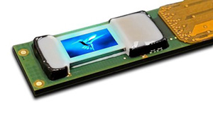
Compound Photonics US Corporation (CP), a global leader providing compact high-resolution microdisplay solutions for Augmented and Mixed Reality (AR/MR), announces today the wide availability of its high-performance digital backplane to leading microLED developers worldwide for integration into complete microdisplay subsystems.
CP re-engineered its market-ready LCoS backplane technology into an innovative constant current drive configuration for microLED pixels based on its industry-leading 0.26” diagonal (~3 ?m pixel) 1080p display format. microLED developers can accelerate their time to market by bonding their devices to a backplane driven by CP’s field-proven NOVA display drive architecture to enable complete display subsystems meeting critical AR requirements for compactness, optical performance and brightness with high frame rate, low latency and low power consumption.
“Our custom, constant current pixel circuit design provides greater tolerance to forward voltage variation and IR drops in the microLED array resulting in a previously unattainable level of uniformity. It additionally features globally on-the-fly programmable pixel current control that greatly increases the system bandwidth, enabling higher frame rates while maintaining full bit depth,” commented Ian Kyles, CP Vice President of Electrical/Software Engineering. “The backplane also has additional steering pixels beyond its native 2048x1080 resolution to enhance alignment/integration of the display within the optical system.”
MicroLED developers using this backplane can access CP’s monolithic integrated display module (IDM) (7.25 x 15.5 x 3.1 mm) with a low pin count interconnect and a direct MIPI input packaged into a compact subsystem amenable to smaller optical engine size. The IDM integrates CP’s proprietary NOVA drive architecture’s software defined platform to enable customizable frame-by-frame control of video frame rates (up to 240 Hz), bit depth, and other parameters to optimize for low latency, short persistence and low power while maintaining near 100% duty cycle according to type of image content and use case.
Andrew Shih, CP’s Marketing and Business Development Manager continued, “Process integration compatibility is also important, as bonding of the microLED array to the backplane requires a highly planar interface. CP’s backplane wafers feature excellent planarity, a direct benefit from extensive process tuning work to meet earlier LCoS requirements. By partnering with CP, whose backplane technology facilitates both wafer level process integration and a direct path to a complete NOVA-based microdisplay subsystem solution, microLED developers can focus on their core competencies in compound semiconductor photonic device engineering and process development while reducing development time and cost.”
A provisional backplane reference specification is presently available for customer review and CP is currently accepting engagements with leading microLED developers.


