


 The Hidden Enabler of Autonomous Warfare: Advanced PCB Technologies Behind Defense AI
 It’s Only Common Sense: Stay Curious, My Friends


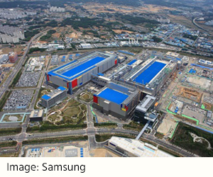
Samsung Electronics Co., Ltd., a world leader in advanced semiconductor technology, today announced plans to boost its foundry capacity at the company's new production line in Pyeongtaek, Korea, to meet growing global demand for cutting-edge extreme ultraviolet (EUV) solutions.
The new foundry line, which will focus on EUV-based 5 nanometer (nm) and below process technology, has just commenced construction this month and is expected to be in full operation in the second half of 2021. It will play a pivotal role as Samsung aims to expand the use of state-of-the-art process technologies across a myriad of current and next generation applications, including 5G, high-performance computing (HPC) and artificial intelligence (AI).
“This new production facility will expand Samsung’s manufacturing capabilities for sub-5nm process and enable us to rapidly respond to the increasing demand for EUV-based solutions,” said Dr. ES Jung, President and Head of Foundry Business at Samsung Electronics. “We remain committed to addressing the needs of our customers through active investments and recruitment of talents. This will enable us to continue to break new ground while driving robust growth for Samsung’s foundry business.”
Following the initial mass production of the EUV-based 7nm process in early 2019, Samsung recently added a new EUV-dedicated V1 line in Hwaseong, Korea, to its global foundry network. With the new Pyeongtaek facility starting full operation in 2021, Samsung’s foundry capacity based on EUV is expected to increase significantly.
Samsung is scheduled to start mass production of 5nm EUV process in the Hwaseong fab in the second half of this year.
With the addition of the Pyeongtaek fab, Samsung will have a total of seven foundry production lines located in South Korea and the United States, comprised of six 12-inch lines and one 8-inch line.


