


 Beyond the Board: Early Engagement Means Faster Prototyping for Defense Programs
 Defense Speak Interpreted: The Autonomous Plane Battle—Skyborg Vs. Loyal Wingman
 American Made Advocacy: Congress Back from Break With Work To Do


Engineers Put Tens of Thousands of Artificial Brain Synapses on a Single Chip
June 9, 2020 | MIT News OfficeEstimated reading time: 5 minutes
The design could advance the development of small, portable AI devices
Jennifer Chu | MIT News Office
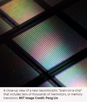
MIT engineers have designed a “brain-on-a-chip,” smaller than a piece of confetti, that is made from tens of thousands of artificial brain synapses known as memristors — silicon-based components that mimic the information-transmitting synapses in the human brain.
The researchers borrowed from principles of metallurgy to fabricate each memristor from alloys of silver and copper, along with silicon. When they ran the chip through several visual tasks, the chip was able to “remember” stored images and reproduce them many times over, in versions that were crisper and cleaner compared with existing memristor designs made with unalloyed elements.
Their results, published today in the journal Nature Nanotechnology, demonstrate a promising new memristor design for neuromorphic devices — electronics that are based on a new type of circuit that processes information in a way that mimics the brain’s neural architecture. Such brain-inspired circuits could be built into small, portable devices, and would carry out complex computational tasks that only today’s supercomputers can handle.
“So far, artificial synapse networks exist as software. We’re trying to build real neural network hardware for portable artificial intelligence systems,” says Jeehwan Kim, associate professor of mechanical engineering at MIT. “Imagine connecting a neuromorphic device to a camera on your car, and having it recognize lights and objects and make a decision immediately, without having to connect to the internet. We hope to use energy-efficient memristors to do those tasks on-site, in real-time.”
Wandering ions
Memristors, or memory transistors, are an essential element in neuromorphic computing. In a neuromorphic device, a memristor would serve as the transistor in a circuit, though its workings would more closely resemble a brain synapse — the junction between two neurons. The synapse receives signals from one neuron, in the form of ions, and sends a corresponding signal to the next neuron.
A transistor in a conventional circuit transmits information by switching between one of only two values, 0 and 1, and doing so only when the signal it receives, in the form of an electric current, is of a particular strength. In contrast, a memristor would work along a gradient, much like a synapse in the brain. The signal it produces would vary depending on the strength of the signal that it receives. This would enable a single memristor to have many values, and therefore carry out a far wider range of operations than binary transistors.
Like a brain synapse, a memristor would also be able to “remember” the value associated with a given current strength, and produce the exact same signal the next time it receives a similar current. This could ensure that the answer to a complex equation, or the visual classification of an object, is reliable — a feat that normally involves multiple transistors and capacitors.
Ultimately, scientists envision that memristors would require far less chip real estate than conventional transistors, enabling powerful, portable computing devices that do not rely on supercomputers, or even connections to the Internet.
Existing memristor designs, however, are limited in their performance. A single memristor is made of a positive and negative electrode, separated by a “switching medium,” or space between the electrodes. When a voltage is applied to one electrode, ions from that electrode flow through the medium, forming a “conduction channel” to the other electrode. The received ions make up the electrical signal that the memristor transmits through the circuit. The size of the ion channel (and the signal that the memristor ultimately produces) should be proportional to the strength of the stimulating voltage.
Kim says that existing memristor designs work pretty well in cases where voltage stimulates a large conduction channel, or a heavy flow of ions from one electrode to the other. But these designs are less reliable when memristors need to generate subtler signals, via thinner conduction channels.
The thinner a conduction channel, and the lighter the flow of ions from one electrode to the other, the harder it is for individual ions to stay together. Instead, they tend to wander from the group, disbanding within the medium. As a result, it’s difficult for the receiving electrode to reliably capture the same number of ions, and therefore transmit the same signal, when stimulated with a certain low range of current.
Borrowing from metallurgy
Kim and his colleagues found a way around this limitation by borrowing a technique from metallurgy, the science of melding metals into alloys and studying their combined properties.
“Traditionally, metallurgists try to add different atoms into a bulk matrix to strengthen materials, and we thought, why not tweak the atomic interactions in our memristor, and add some alloying element to control the movement of ions in our medium,” Kim says.
Engineers typically use silver as the material for a memristor’s positive electrode. Kim’s team looked through the literature to find an element that they could combine with silver to effectively hold silver ions together, while allowing them to flow quickly through to the other electrode.
The team landed on copper as the ideal alloying element, as it is able to bind both with silver, and with silicon.
“It acts as a sort of bridge, and stabilizes the silver-silicon interface,” Kim says.
To make memristors using their new alloy, the group first fabricated a negative electrode out of silicon, then made a positive electrode by depositing a slight amount of copper, followed by a layer of silver. They sandwiched the two electrodes around an amorphous silicon medium. In this way, they patterned a millimeter-square silicon chip with tens of thousands of memristors.
As a first test of the chip, they recreated a gray-scale image of the Captain America shield. They equated each pixel in the image to a corresponding memristor in the chip. They then modulated the conductance of each memristor that was relative in strength to the color in the corresponding pixel.
The chip produced the same crisp image of the shield, and was able to “remember” the image and reproduce it many times, compared with chips made of other materials.
The team also ran the chip through an image processing task, programming the memristors to alter an image, in this case of MIT’s Killian Court, in several specific ways, including sharpening and blurring the original image. Again, their design produced the reprogrammed images more reliably than existing memristor designs.
“We’re using artificial synapses to do real inference tests,” Kim says. “We would like to develop this technology further to have larger-scale arrays to do image recognition tasks. And some day, you might be able to carry around artificial brains to do these kinds of tasks, without connecting to supercomputers, the internet, or the cloud.”
This research was funded, in part, by the MIT Research Support Committee funds, the MIT-IBM Watson AI Lab, Samsung Global Research Laboratory, and the National Science Foundation.
Read the original article here.
Share on:


Testimonial
"We’re proud to call I-Connect007 a trusted partner. Their innovative approach and industry insight made our podcast collaboration a success by connecting us with the right audience and delivering real results."
Julia McCaffrey - NCAB GroupSuggested Items
Episode 6 of Ultra HDI Podcast Series Explores Copper-filled Microvias in Advanced PCB Design and Fabrication
10/15/2025 | I-Connect007I-Connect007 has released Episode 6 of its acclaimed On the Line with... American Standard Circuits: Ultra High Density Interconnect (UHDI) podcast series. In this episode, “Copper Filling of Vias,” host Nolan Johnson once again welcomes John Johnson, Director of Quality and Advanced Technology at American Standard Circuits, for a deep dive into the pros and cons of copper plating microvias—from both the fabricator’s and designer’s perspectives.
Nolan’s Notes: Tariffs, Technologies, and Optimization
10/01/2025 | Nolan Johnson -- Column: Nolan's NotesLast month, SMT007 Magazine spotlighted India, and boy, did we pick a good time to do so. Tariff and trade news involving India was breaking like a storm surge. The U.S. tariffs shifted India from one of the most favorable trade agreements to the least favorable. Electronics continue to be exempt for the time being, but lest you think that we’re free and clear because we manufacture electronics, steel and aluminum are specifically called out at the 50% tariff levels.
MacDermid Alpha & Graphic PLC Lead UK’s First Horizontal Electroless Copper Installation
09/30/2025 | MacDermid Alpha & Graphic PLCMacDermid Alpha Electronics Solutions, a leading supplier of integrated materials and chemistries to the electronics industry, is proud to support Graphic PLC, a Somacis company, with the installation of the first horizontal electroless copper metallization process in the UK.
Electrodeposited Copper Foils Market to Grow by $11.7 Billion Over 2025-2032
09/18/2025 | Globe NewswireThe global electrodeposited copper foils market is poised for dynamic growth, driven by the rising adoption in advanced electronics and renewable energy storage solutions.
MacDermid Alpha Showcases Advanced Interconnect Solutions at PCIM Asia 2025
09/18/2025 | MacDermid Alpha Electronics SolutionsMacDermid Alpha Electronic Solutions, a global leader in materials for power electronics and semiconductor assembly, will showcase its latest interconnect innovations in electronic interconnect materials at PCIM Asia 2025, held from September 24 to 26 at the Shanghai New International Expo Centre, Booth N5-E30