


 The Marketing Minute: If Your Marketing Budget Gets Cut in Half, Then What?
 Punching Out: How Are the Big Boys in Electronics Doing?
 It’s Only Common Sense: Complexity Is the Enemy of Profit


Isola Opens Expanded R&D and Analytical Laboratory in Arizona
June 19, 2020 | PR NewswireEstimated reading time: 2 minutes
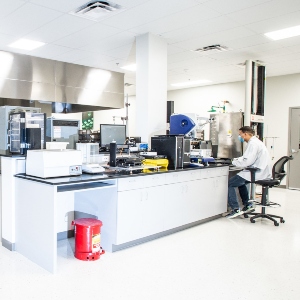
Isola, designer and developer of copper-clad laminates and fabrication materials for multi-layer printed circuit boards (PCBs), has officially opened an expansive R&D and analytical services laboratory at the company's new global headquarters in Chandler, Ariz.
Nearly doubling the size and capacity of the testing facility enables enhanced product development, material qualification, application engineering, and technical support to printed circuit board fabricators and the OEMs they serve. Access to Isola's testing facilities throughout the world is a complimentary service offered to Isola customers. The Arizona operations also include a 118,000-square-foot quick-turnaround manufacturing facility to accommodate the industry's agile demands.
In the R&D and analytical lab, Isola incorporated a refined and optimized workflow with dedicated space for each testing process. These dedicated spaces provide a more optimal working environment for Isola technicians, chemists, and researchers, benefiting customers through enhanced efficiency. The lab's highly trained team conducts electrical, thermal, and mechanical characterizations of resin components and PCB laminate materials used in the production of printed circuit boards and uses advanced test equipment to achieve accurate results in a rapid response environment. Known as the Johann Schumacher Laboratories, the facility is named for an Isola technical fellow and engineer, who—throughout his 35 years with the company—has developed numerous innovations.
"The North American PCB market is all about quick turnaround and high complexity. Isola's investment in local testing and analysis complements the investments our customers have made to meet the growing complexity of the products designed by OEMs," said Travis Kelly, President & CEO. "The expanded R&D and analytical services laboratory furthers our ability to both improve analytical capability and maintain quick turnaround times."
The lab includes a variety of testing equipment—from Fourier Transform Infrared Spectroscopy (FTIR) and Scanning Electron Microscopy (SEM) analysis for identification of contaminants to microsection equipment used for evaluation of printed circuit board integrity after thermal excursions. The thermal analysis area consists of 17 instruments that measure thermal properties as a function of temperature while specimens are subject to a controlled temperature program.
"While thermal analysis is one of the lab's most in-demand services, the global Johann Schumacher Laboratories network, with locations in the U.S., Singapore, and Germany, helps customers work through various challenges related to their products," said Jenny Inocencio, Sr. Manager Global JSL. "Our cross-trained professionals—many of whom also have experience in the manufacturing environment—understand the full process of how materials are assembled, bring keen insights to identifying problems, and confidently consider different approaches. Customers have the advantage of leveraging our global network as their business needs change and during unexpected market events."
Isola's global R&D and analytical laboratory team is led by Ed Kelley, Chief Technology Officer, Phil Whalen, Chief New Product Development and Strategy Officer, Drew Rocha, R&D Manager; and Jenny Inocencio, Senior Manager, Global JSL
Share on:


Testimonial
"In a year when every marketing dollar mattered, I chose to keep I-Connect007 in our 2025 plan. Their commitment to high-quality, insightful content aligns with Koh Young’s values and helps readers navigate a changing industry. "
Brent Fischthal - Koh YoungSuggested Items
I-Connect007 Releases The Printed Circuit Designer’s Guide to… Direct Metallization: A Guide to Complex PCB Fabrication
05/13/2026 | I-Connect007As PCB complexity continues to accelerate, fabricators and OEMs are reevaluating long-standing manufacturing processes to meet the demands of AI, HDI, advanced packaging, and next-generation electronics. To address these evolving challenges, I-Connect007 is proud to announce the release of The Printed Circuit Designer’s Guide to… Direct Metallization: A Guide to Complex PCB Fabrication, authored by MacDermid Alpha Solution’s Carmichael Gugliotti.
Driving Innovation: Selecting the Right Laser Source
04/28/2026 | Simon Khesin -- Column: Driving InnovationWhen I first joined Schmoll Maschinen, I brought experience from almost every PCB process, except for laser. As I immersed myself in laser processing, I realized why it can seem so daunting to a newcomer. The complexity arises from three intersecting factors: A vast variety of laser sources: CO2, UV-nano, green-pico, UV-pico, IR-pico, and others; a diverse range of applications: Drilling, cutting, ablation, and more; and an extensive list of materials: These have vastly different absorption rates. Choosing the right machine or laser source is rarely trivial. Even for experienced engineers, answering "Which source is best?" requires examining the business's specific goals.
Institute of Circuit Technology Spring Seminar 2026: A Bright Future in Europe
04/23/2026 | Pete Starkey, I-Connect007Through the leafy lanes and spring flowers of Warwickshire and back to Meridan, the traditional centre of England, and now officially part of the Metropolitan Borough of Solihull in the county of the West Midlands, I attended the Annual General Meeting and Spring Seminar of the Institute of Circuit Technology (ICT) on April 14. Out of the AGM came notable changes in leadership at the top of the Institute: the retirement of Mat Beadel as chair and Emma Hudson as technical director. Effective May 1, Steve Driver is the new chair, and Alun Morgan is the new technical director.
ACCM Unveils Negative and Near-zero CTE Materials for Large-Format AI Chips
04/21/2026 | Advanced Chip and Circuit MaterialsAdvanced Chip and Circuit Materials, Inc. (ACCM) has launched two new materials: Celeritas HM50, with a negative coefficient of thermal expansion (CTE) of -8 ppm/°C to offset the positive CTE and expansion of copper with temperature on circuit boards, and Celeritas HM001, with near-zero CTE and the low-loss performance needed for high-speed signal layers to 224 Gb/s and faster in artificial intelligence (AI) circuits.
Fresh PCB Concepts: Designing PCBs for Harsh Environments—Reliability Is Engineered Upstream
04/23/2026 | Team NCAB -- Column: Fresh PCB ConceptsWhen engineers hear the phrase “harsh environment,” they usually think of the extreme temperature swings, vibration and shock, pressure changes, or radiation in aerospace. However, aerospace is not the only harsh environment where electronic assemblies must survive. Automotive power electronics, downhole oil and gas tools, marine controls, rail systems, defense platforms, and industrial automation equipment all expose PCBs to environments that are equally unforgiving. The stress mechanisms may differ, but the physics does not.