


 The Marketing Minute: If Your Marketing Budget Gets Cut in Half, Then What?
 Punching Out: How Are the Big Boys in Electronics Doing?
 It’s Only Common Sense: Complexity Is the Enemy of Profit


Ventec International Group Celebrates 10th Anniversary of German Subsidiary
October 15, 2020 | Ventec International GroupEstimated reading time: 3 minutes
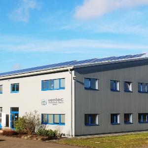
Ventec International Group is pleased to celebrate the 10th anniversary of its wholly owned subsidiary Ventec Europe GmbH in Kirchheimbolanden, Germany. Since its formation on 27th October 2010, the German facility has grown into a state-of-the-art operation offering warehousing & distribution, sales & technical service expertise and quick turn manufacturing capabilities including an ISO 7 (Class 10000) clean room for prepreg panel fabrication.
Ventec Europe GmbH was established in 2010 to support Ventec International Group’s global operations as an integral part of the company’s fully controlled and managed global supply chain, sales- and technical support-network. Driven by demand from high reliability automotive, medical, military and aerospace applications, Ventec’s Central European manufacturing & distribution center in Germany, has grown into a key strategic quick turn fabrication and distribution hub for customers in Europe, the Middle East and Africa.
Over the past decade, the facility has expanded through continuous investment by its parent company which is dedicated to consistently providing and maintaining meticulous aerospace-standard cleanliness in Germany and key locations around the world. Today, the ISO 9001-certified prepreg and laminate handling facility (supplemented by the company’s main manufacturing site certifications of AS9100 Rev D for aerospace and IATF 16949:2016 for automotive certifications), boasts a fully upgraded 650sqm dedicated laminate cutting room with state-of-the-art extraction fittings, two diamond blade saws and an immaculately presented, upgraded temperature & humidity-controlled ISO 7 (Class 10000) clean-room for epoxy prepreg cutting and packing. The Pasquato slitter/sheeter within the clean-room has a constant laminar down-flow of highly filtered air to give an ultra-clean operating environment with real-time monitoring of temperature and humidity.
With 5G driving even greater demand for high-performance formulations characterized by very low losses, Ventec is now ramping up to support PCB manufacturers in this key transformation process. Mark Goodwin, COO Europe & America explained: “5G and applications like 77GHz automotive radar are set for explosive growth and are calling for ever more technically specialized materials. Tightly controlled dielectric constant and low dissipation factor are needed to ensure signal integrity and minimize power demand and heat dissipation. Low passive intermodulation and good thermal stability are also required. At Ventec, our advanced tec-speed and tec-thermal materials will make the difference in achieving our customers’ technical requirements for the 5G revolution.”
Frank Lorentz, Internal General Manager at Ventec’s German facility continued: “As an integral part of our state-of-the-art facilities around the world, and supported by an excellent team, our facility in Germany ensures that we maintain the high quality of solutions and services that are witnessing increasing demand across our client base in Europe and beyond. As we celebrate the 10th anniversary, my heartfelt gratitude goes out to our loyal customers for their continued support and the great team here and across the Ventec family for their dedication and hard work without whom the exponential growth and tremendous success of Ventec would not have been possible.”
Ventec International is a world leader in the production of polyimide & high reliability epoxy laminates and prepregs and specialist provider of thermal management and IMS solutions. Further information about Ventec’s solutions and the company’s wide variety of products is available at www.venteclaminates.com and/or by downloading the Ventec APP.
About Ventec International Group
Ventec International is a premier supplier to the Global PCB industry. With volume manufacturing facilities in Taiwan and China and distribution locations and manufacturing sites in both the US and Europe, Ventec specializes in advanced copper clad glass reinforced and metal backed substrates. Ventec materials, which include high-quality enhanced FR4, high-speed/low-loss- & high-performance IMS material technology and an advanced range of thermal management solutions, are manufactured by Ventec using strict quality-controlled processes that are certified to AS9100 Revision D, IATF 16949:2016 and ISO 9001:2015, and are backed by a fully controlled and managed global supply chain, sales- and technical support-network.
Share on:


Testimonial
"We’re proud to call I-Connect007 a trusted partner. Their innovative approach and industry insight made our podcast collaboration a success by connecting us with the right audience and delivering real results."
Julia McCaffrey - NCAB GroupSuggested Items
I-Connect007 Releases The Printed Circuit Designer’s Guide to… Direct Metallization: A Guide to Complex PCB Fabrication
05/13/2026 | I-Connect007As PCB complexity continues to accelerate, fabricators and OEMs are reevaluating long-standing manufacturing processes to meet the demands of AI, HDI, advanced packaging, and next-generation electronics. To address these evolving challenges, I-Connect007 is proud to announce the release of The Printed Circuit Designer’s Guide to… Direct Metallization: A Guide to Complex PCB Fabrication, authored by MacDermid Alpha Solution’s Carmichael Gugliotti.
Driving Innovation: Selecting the Right Laser Source
04/28/2026 | Simon Khesin -- Column: Driving InnovationWhen I first joined Schmoll Maschinen, I brought experience from almost every PCB process, except for laser. As I immersed myself in laser processing, I realized why it can seem so daunting to a newcomer. The complexity arises from three intersecting factors: A vast variety of laser sources: CO2, UV-nano, green-pico, UV-pico, IR-pico, and others; a diverse range of applications: Drilling, cutting, ablation, and more; and an extensive list of materials: These have vastly different absorption rates. Choosing the right machine or laser source is rarely trivial. Even for experienced engineers, answering "Which source is best?" requires examining the business's specific goals.
Institute of Circuit Technology Spring Seminar 2026: A Bright Future in Europe
04/23/2026 | Pete Starkey, I-Connect007Through the leafy lanes and spring flowers of Warwickshire and back to Meridan, the traditional centre of England, and now officially part of the Metropolitan Borough of Solihull in the county of the West Midlands, I attended the Annual General Meeting and Spring Seminar of the Institute of Circuit Technology (ICT) on April 14. Out of the AGM came notable changes in leadership at the top of the Institute: the retirement of Mat Beadel as chair and Emma Hudson as technical director. Effective May 1, Steve Driver is the new chair, and Alun Morgan is the new technical director.
ACCM Unveils Negative and Near-zero CTE Materials for Large-Format AI Chips
04/21/2026 | Advanced Chip and Circuit MaterialsAdvanced Chip and Circuit Materials, Inc. (ACCM) has launched two new materials: Celeritas HM50, with a negative coefficient of thermal expansion (CTE) of -8 ppm/°C to offset the positive CTE and expansion of copper with temperature on circuit boards, and Celeritas HM001, with near-zero CTE and the low-loss performance needed for high-speed signal layers to 224 Gb/s and faster in artificial intelligence (AI) circuits.
Fresh PCB Concepts: Designing PCBs for Harsh Environments—Reliability Is Engineered Upstream
04/23/2026 | Team NCAB -- Column: Fresh PCB ConceptsWhen engineers hear the phrase “harsh environment,” they usually think of the extreme temperature swings, vibration and shock, pressure changes, or radiation in aerospace. However, aerospace is not the only harsh environment where electronic assemblies must survive. Automotive power electronics, downhole oil and gas tools, marine controls, rail systems, defense platforms, and industrial automation equipment all expose PCBs to environments that are equally unforgiving. The stress mechanisms may differ, but the physics does not.