-

-
News
News Highlights
- Books
Featured Books
- smt007 Magazine
Latest Issues
Current Issue
Spotlight on Mexico
Mexico isn’t just part of the electronics manufacturing conversation—it’s leading it. From growing investments to cross-border collaborations, Mexico is fast becoming the center of electronics in North America. This issue includes bilingual content, with all feature articles available in both English and Spanish.

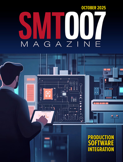
Production Software Integration
EMS companies need advanced software systems to thrive and compete. But these systems require significant effort to integrate and deploy. What is the reality, and how can we make it easier for everyone?

Spotlight on India
We invite you on a virtual tour of India’s thriving ecosystem, guided by the Global Electronics Association’s India office staff, who share their insights into the region’s growth and opportunities.
- Articles
- Columns
- Links
- Media kit
||| MENU - smt007 Magazine
SelecTech Announces Banner Year in 2020
January 8, 2021 | SelecTechEstimated reading time: 1 minute
StaticStop, a division of SelecTech, Inc., and leader in the manufacture of innovative ESD flooring products that save time and money, has announced that 2020 was a banner year for the company with 10% growth.
“2020 certainly offered many challenges,” commented Tom Ricciardelli, President of SelecTech. “I’m proud to say despite COVID, travel restrictions and all the other curveballs the year threw at us, we were able to increase sales 10%. By working hand in hand with our sales partners, we developed new content, offered learning courses, and supported their efforts with blog and email campaigns, helping us sell more flooring.”
StaticStop is a division of SelecTech, Inc., which was founded in 1993 with the mission of creating valuable products from scrap plastics. The company is a leader in the manufacture of flooring products from recycled materials and uses one million pounds of recycled materials annually. Their FreeStyle ESD and SelecTile ESD products are made with recycled content and are 100 percent recyclable. Both FreeStyle ESD and SelecTile ESD are installed without adhesives making them some of the “greenest” and most cost-effective flooring products available.
FreeStyle ESD™ is the first and only decorative flooring system that is “conductive, connected and grounded”™. This unique and innovative flooring solution is easy to install without the need for messy adhesives, copper foil, underlayments or padding. This simplified and convenient installation process translates into less down time for your facility, further translating into reduced costs and an improved bottom line. Additionally, these floor tiles DO NOT require any conductive rejuvenators, wax, or expensive maintenance solutions.
SelecTile ESD™ flooring is a free-floating surface with a unique interlocking tab system. These static-control flooring products install quickly and easily without the need for adhesives, copper strips, underlayments or padding. StaticStops’s static-control systems were uniquely engineered to meet the demanding needs of industrial environments that require the highest level of electrostatic discharge protection, and still withstand industrial environments, including fork truck traffic. StaticStop offers a truly robust system that is completely scalable to any specification or intricate layout.
Testimonial
"In a year when every marketing dollar mattered, I chose to keep I-Connect007 in our 2025 plan. Their commitment to high-quality, insightful content aligns with Koh Young’s values and helps readers navigate a changing industry. "
Brent Fischthal - Koh YoungSuggested Items
WestDev Announces Advanced Thermal Analysis Integration for Pulsonix PCB Design Suite
10/29/2025 | WestDev Ltd.Pulsonix, the industry-leading PCB design software from WestDev Ltd., announced a major enhancement to its design ecosystem: a direct interface between Pulsonix and ADAM Research's TRM (Thermal Risk Management) analysis software.
Designers Notebook: Power and Ground Distribution Basics
10/29/2025 | Vern Solberg -- Column: Designer's NotebookThe principal objectives to be established during the planning stage are to define the interrelationship between all component elements and confirm that there is sufficient surface area for placement, the space needed to ensure efficient circuit interconnect, and to accommodate adequate power and ground distribution.
Episode 6 of Ultra HDI Podcast Series Explores Copper-filled Microvias in Advanced PCB Design and Fabrication
10/15/2025 | I-Connect007I-Connect007 has released Episode 6 of its acclaimed On the Line with... American Standard Circuits: Ultra High Density Interconnect (UHDI) podcast series. In this episode, “Copper Filling of Vias,” host Nolan Johnson once again welcomes John Johnson, Director of Quality and Advanced Technology at American Standard Circuits, for a deep dive into the pros and cons of copper plating microvias—from both the fabricator’s and designer’s perspectives.
Nolan’s Notes: Tariffs, Technologies, and Optimization
10/01/2025 | Nolan Johnson -- Column: Nolan's NotesLast month, SMT007 Magazine spotlighted India, and boy, did we pick a good time to do so. Tariff and trade news involving India was breaking like a storm surge. The U.S. tariffs shifted India from one of the most favorable trade agreements to the least favorable. Electronics continue to be exempt for the time being, but lest you think that we’re free and clear because we manufacture electronics, steel and aluminum are specifically called out at the 50% tariff levels.
MacDermid Alpha & Graphic PLC Lead UK’s First Horizontal Electroless Copper Installation
09/30/2025 | MacDermid Alpha & Graphic PLCMacDermid Alpha Electronics Solutions, a leading supplier of integrated materials and chemistries to the electronics industry, is proud to support Graphic PLC, a Somacis company, with the installation of the first horizontal electroless copper metallization process in the UK.


