-

- News
- Books
Featured Books
- smt007 Magazine
Latest Issues
Current Issue
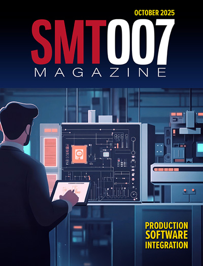
Production Software Integration
EMS companies need advanced software systems to thrive and compete. But these systems require significant effort to integrate and deploy. What is the reality, and how can we make it easier for everyone?

Spotlight on India
We invite you on a virtual tour of India’s thriving ecosystem, guided by the Global Electronics Association’s India office staff, who share their insights into the region’s growth and opportunities.

Supply Chain Strategies
A successful brand is built on strong customer relationships—anchored by a well-orchestrated supply chain at its core. This month, we look at how managing your supply chain directly influences customer perception.
- Articles
- Columns
- Links
- Media kit
||| MENU - smt007 Magazine
Best Practices: Footprint Design and CAD Library Management
February 9, 2021 | I-Connect007 Editorial TeamEstimated reading time: 2 minutes
The I-Connect team spoke with Altium’s John Watson about the hurdles surrounding footprints and footprint design. John talks about how being proactive and improving the CAD library can better QC processes and help protect against footprint difficulties.
Andy Shaughnessy: I’m here today with John Watson from Altium to discuss footprints, footprint design, and what can be done to achieve best practices. This came about because we recently conducted surveys asking for design problems. The results came mainly from designers, and around a quarter of them said footprint issues were a big problem.
John Watson: There’s a real conflict in a lot of companies. They want to get their product to market. So, I think that the first issue that comes in with anything in a design is this conflict between the management schedule and the design schedule. If you’re creating a new component, for example, number one is that component needs to be put into quarantine. It’s not used in new designs. It needs to be put into quarantine and checked. There’s such a rush to say, “We’ve got to get this done and get it out.” And there’s just too much going on in a design to catch things that are wrong like that.
Barry Matties: How long should it be in quarantine?
Watson: It stays in quarantine until a couple of processes are completed. Number one, there is a QC process that’s done on that component, and that QC process is actually multi-level. There will be different steps involved. For example, if you have a new component, you bring that component in or that footprint in, and you verify that footprint to the datasheet. On this first level of QC, you want to set up your verification documents to that footprint. What are we going to be looking at? We’re going to be comparing this footprint to the datasheet, we’re going to be looking at IPC standards, whatever the standards are that you’re going to be lining this footprint up with. That’s going to be your first level of QC, but I’ve actually seen where there’s a second level of QC that’s done. Once that part has been verified to the datasheet, that part then goes into what’s called the prototype status; what it does is that component is then put onto a PCB, kind of a live test.
When that board comes back with the component on it, you look at it under the scope to see if there are any issues with the soldering. It’s like a real-world environment. Those are the two levels of QC. Number one, you compare it to the documentation, and then you have a real-world environment that you take it through. That step and those processes are what you go through. That way, you’ve actually had both sides of it: You have your side of it, and then also the assembler’s side of it. I’ve found that a lot of times, believe it or not—I know it’s a shocking comment I’m about to make—but datasheets have been known to be wrong. VPs have no understanding of what it takes to put a PCB design out—the steps, the checks that you have to do, all these different things. Often, that’s lost in this whole process.
To read this entire conversation, which appeared in the February 2021 issue of Design007 Magazine, click here.
Testimonial
"We’re proud to call I-Connect007 a trusted partner. Their innovative approach and industry insight made our podcast collaboration a success by connecting us with the right audience and delivering real results."
Julia McCaffrey - NCAB GroupSuggested Items
Peters, Starteam, and Würth Elektronik Team Up For Digital Coating Technology
10/23/2025 | PetersUnder this heading, the PCB manufacturers Starteam and Würth Elektronik, along with Peters as inkjet coating supplier, have taken the initiative and worked together for months in trusting and target-oriented cooperation, to promote this innovative digital coating technology for solder resists and establish it on the market.
AI Triggers Next Paradigm Shift in PDN
10/23/2025 | Istvan Novak, SamtecArtificial intelligence (AI), together with machine learning (ML), is creating an unprecedented surge of computing and networking infrastructure needs. This, in turn, has dramatically increased the power consumption of computing and networking chips.
SEMICON Japan 2025 to Spotlight Sustainability in AI and Semiconductor Innovation
10/22/2025 | SEMISEMICON Japan 2025, the largest gathering of leaders from the microelectronics manufacturing supply chain in Japan, will bring together more than 1,200 exhibitors showcasing semiconductor solutions from December 17-19 at Tokyo Big Sight.
Zuken Announces ZIW Americas 2026 in Dallas
10/21/2025 | ZukenZuken USA, Inc., a global leader in electrical and electronic design automation, announced Zuken Innovation World (ZIW) Americas 2026, the company’s premier global conference dedicated to advancing the future of electrical and electronic product design. ZIW 2026 will be held June 9-11 in Dallas, Texas.
Keysight Completes Acquisition of Synopsys’ Optical Solutions Group and Ansys’ PowerArtist
10/17/2025 | Keysight Technologies, Inc.Keysight Technologies, Inc., announced the completion of its acquisitions of the Optical Solutions Group from Synopsys, Inc., and PowerArtist from Ansys, Inc.


