-
- News
- Books
Featured Books
- pcb007 Magazine
Latest Issues
Current IssueInventing the Future with SEL
Two years after launching its state-of-the-art PCB facility, SEL shares lessons in vision, execution, and innovation, plus insights from industry icons and technology leaders shaping the future of PCB fabrication.
Sales: From Pitch to PO
From the first cold call to finally receiving that first purchase order, the July PCB007 Magazine breaks down some critical parts of the sales stack. To up your sales game, read on!
The Hole Truth: Via Integrity in an HDI World
From the drilled hole to registration across multiple sequential lamination cycles, to the quality of your copper plating, via reliability in an HDI world is becoming an ever-greater challenge. This month we look at “The Hole Truth,” from creating the “perfect” via to how you can assure via quality and reliability, the first time, every time.
- Articles
- Columns
- Links
- Media kit
||| MENU - pcb007 Magazine
Kuprion Introduces ActiveCopper Filled Thermal Vias
February 12, 2021 | Kuprion, Inc.Estimated reading time: 2 minutes

Kuprion, Inc., a spinout of Lockheed Martin, has introduced ActiveCopper™ Filled Thermal Vias, leveraging a patented technology breakthrough that addresses the increased reliability demands of heat and power dissipation for complex, advanced high performance systems.
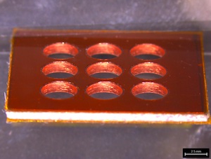
Lead-free and RoHs-compliant, ActiveCopper is a flowable, engineered copper paste—a dense and sticky form of copper, which is safe to handle in air. To enhance heat and power dissipation, ActiveCopper Filled Thermal Vias provide a more efficient heat dissipation path directly incorporated into PCBs with placement directly under a surface-mounted IC ‘heat source’ that allows direct surface mount bonding for maximum heat transfer using Kuprion’s surface mount copper material. Placing the large 3-5mm diameter thermal vias directly underneath an IC allows direct bonding to such a via, and enables significant reduction in thermal resistance. This facilitates efficient heat dissipation not only on the top surface, but through the PCB to the back side.
“The heat generated by integrated circuits poses great challenges, especially given today’s faster speeds, reduced board real estate and the multitude of devices being populated on PCBs. These demands require more efficient methods of heat and power dissipation to ensure product performance and life for increasingly complex electronic systems,” stated Nick Antonopoulos, CEO at Kuprion. “The PCB by nature, like common FR4 material, is not a good thermal conductor. It’s made of substrate materials that are insulating electrical interconnections between components, but ActiveCopper Filled Thermal Vias provides an ideal solution.”
Kuprion’s Active Cu (ActiveCopper) Thermal Via paste is easily applied by printing, or squeegeeing into these vias, where it is converted into bulk copper during processing. This allows for thermal conductivity of at least 150 W m-1 K-1, and fills holes from micro vias to 4+ mm diameter vias while sintering at approximately 200°C. Additionally, there is no re-melting after sintering, allowing for unlimited reflow sequences.
ActiveCopper Filled Thermal Vias are ideal for advanced high power/high performance applications such as 5G transreceivers/power amplifiers, industrial LEDs, graphics cards, data servers, routers, and automotive lighting with the following advantages:
- Lead-free, RoHs-compliant; nearly 100 percent densified bulk copper after sintering
- No re-melting after sintering; converts to bulk copper (m.p. 1084°C)
- Enables unlimited reflow sequences
- Thermal conductivity: 150 - 160 W m-1 K-1
- Rapid processing: 20 - 40 minutes; no-clean material system
- Proven solution backed by 12+ years of R&D
- Cost-effective and ready for immediate use for a range of global customer applications
Testimonial
"Our marketing partnership with I-Connect007 is already delivering. Just a day after our press release went live, we received a direct inquiry about our updated products!"
Rachael Temple - AlltematedSuggested Items
Trouble in Your Tank: Minimizing Small-via Defects for High-reliability PCBs
08/27/2025 | Michael Carano -- Column: Trouble in Your TankTo quote the comedian Stephen Wright, “If at first you don’t succeed, then skydiving is not for you.” That can be the battle cry when you find that only small-diameter vias are exhibiting voids. Why are small holes more prone to voids than larger vias when processed through electroless copper? There are several reasons.
The Government Circuit: Navigating New Trade Headwinds and New Partnerships
08/25/2025 | Chris Mitchell -- Column: The Government CircuitAs global trade winds continue to howl, the electronics manufacturing industry finds itself at a critical juncture. After months of warnings, the U.S. Government has implemented a broad array of tariff increases, with fresh duties hitting copper-based products, semiconductors, and imports from many nations. On the positive side, tentative trade agreements with Europe, China, Japan, and other nations are providing at least some clarity and counterbalance.
How Good Design Enables Sustainable PCBs
08/21/2025 | Gerry Partida, Summit InterconnectSustainability has become a key focus for PCB companies seeking to reduce waste, conserve energy, and optimize resources. While many discussions on sustainability center around materials or energy-efficient processes, PCB design is an often overlooked factor that lies at the heart of manufacturing. Good design practices, especially those based on established IPC standards, play a central role in enabling sustainable PCB production. By ensuring designs are manufacturable and reliable, engineers can significantly reduce the environmental impact of their products.
50% Copper Tariffs, 100% Chip Uncertainty, and a Truce
08/19/2025 | Andy Shaughnessy, I-Connect007If you’re like me, tariffs were not on your radar screen until a few months ago, but now political rhetoric has turned to presidential action. Tariffs are front-page news with major developments coming directly from the Oval Office. These are not typical times. President Donald Trump campaigned on tariff reform, and he’s now busy revamping America’s tariff policy.
Global PCB Connections: Understanding the General Fabrication Process—A Designer’s Hidden Advantage
08/14/2025 | Markus Voeltz -- Column: Global PCB ConnectionsDesigners don’t need to become fabricators, but understanding the basics of PCB fabrication can save you time, money, and frustration. The more you understand what’s happening on the shop floor, the better you’ll be able to prevent downstream issues. As you move into more advanced designs like HDI, flex circuits, stacked vias, and embedded components, this foundational knowledge becomes even more critical. Remember: the fabricator is your partner.