


 The Marketing Minute: If Your Marketing Budget Gets Cut in Half, Then What?
 Punching Out: How Are the Big Boys in Electronics Doing?
 It’s Only Common Sense: Complexity Is the Enemy of Profit


AT&S Starts Construction of First High-tech Manufacturing Facility in Southeast Asia
October 29, 2021 | AT&SEstimated reading time: 2 minutes
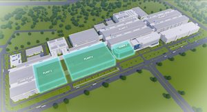
AT&S, one of the globally leading manufacturers of high-end printed circuit boards and IC substrates, headquartered in Austria (Europe), announced detailed project information on the company’s planned investment in a state-of-the-art factory for IC substrates at the Kulim Hi-Tech Park, Kedah.
During a press conference, AT&S CEO Andreas Gerstenmayer and AT&S COO Ingolf Schroeder gave insights into the planned investment, the project scope, technology details, as well as the planned activities to hire approx. 6,000 highly qualified employees.
AT&S’ new campus for the production of IC substrates in Kulim Hi-Tech Park, Kedah, involves a proposed total investment for phase 1 of RM 8.5 billion (€1.7 billion). The construction of the facility is going to start with an official groundbreaking ceremony on October 30, 2021, with commercial operations targeted to come on stream in 2024.
“I want to thank the Malaysian government as well as the MIDA (the government’s principal promotion agency under the Ministry of International Trade and Industry) for the great support throughout the entire process, from the start of our location scouting until today,” says AT&S CEO Andreas Gerstenmayer. “Already today, Malaysia is an important hub for the chip supply chain. We are convinced that Malaysia can further strengthen its position as a technology country and will develop its position in the region as a high-tech manufacturing hub in Asia,” Gerstenmayer says.
Not only will thousands of new jobs be created in the region, but Malaysia will make a name for itself as a hotspot for a completely new, first-of-its-kind technology segment. “AT&S brings the latest generation of high-end technologies to Malaysia and will establish a completely new technology sector in one of the future global microelectronic hotspots. In addition to manufacturing high-tech products, extensive R&D activities will also be conducted at this new site,” AT&S COO Ingolf Schroeder says.
All these activities require a high amount of highly qualified human resources and will boost the region’s labor market. The search profiles for employees at the new AT&S plant range from specialists, managers, and leaders in the areas of electronic, mechanical, and chemical engineers, and business. At the same time, AT&S is also looking for about 4,500 blue-collar workers who can work in a highly sophisticated shop floor environment.
Besides manufacturing, R&D will also be a focus at the new AT&S facility in Kulim. Therefore, AT&S is investigating cooperation and partnerships with leading universities in Malaysia. “These partnerships will not only help us to discover new paths for the microelectronics industry,” Andreas Gerstenmayer says. “They will also make an important contribution to the development of extensive know-how in the various areas of the microelectronics industry for Malaysia and, at the end of the day, contribute to the positive development of the society.”
Share on:


Testimonial
"Advertising in PCB007 Magazine has been a great way to showcase our bare board testers to the right audience. The I-Connect007 team makes the process smooth and professional. We’re proud to be featured in such a trusted publication."
Klaus Koziol - atgSuggested Items
TPCA Launches AI-Powered PCB GPT Knowledge Platform
05/15/2026 | TPCAThe Taiwan Printed Circuit Association (TPCA) has launched the "PCB GPT Industry Knowledge Platform," which uses generative AI to connect PCB professional knowledge services and help the industry improve the efficiency of cross-border and professional talent training.
I-Connect007 Editor’s Choice: Five Must-Reads for the Week
05/15/2026 | Nolan Johnson, I-Connect007When you work in the news business, even in trade media, you can never really get that far away from it. We never want to miss something important. Chances are, even the books we take on our “vacations” end up having to do with the business. For example, my colleague Michelle Te recommended “Creativity, Inc., by Ed Catmull, a business skills study wrapped up in stories about Pixar, which I brought with me on a trip through the stunning U.S. Mountain West. Now, I’m back, and here are my recommendations for the week.
STARTEAM GLOBAL Achieves A Score in CDP’s Supplier Engagement Assessment
05/14/2026 | STARTEAM GLOBALSTARTEAM GLOBAL has achieved an A score in CDP’s Supplier Engagement Assessment (SEA).
Rethinking Stackup, Materials, and Tolerances in Modern Designs
05/14/2026 | Kristin Moyer, Global Electronics AssociationThe simple rectangular rigid PCB is becoming increasingly infrequent. This reality necessitates designing with concepts well outside traditional rigid PCB methodologies. For example, the designer of wearable electronics may need to implement conductive fibers integrated into the textile material. Heads-up displays, like those in VR/AR headsets and glasses, require transparent circuitry etched into the display glass. The process of designing without a rule book usually starts with something other than the traditional board design process.
Separating Fact from Fear on the FCC ‘China Lab Ban’
05/14/2026 | Jan Pedersen, NCAB GroupRecent news headlines have suggested that the U.S. Federal Communications Commission (FCC) has “banned all testing laboratories in China and Hong Kong.” Understandably, this has created concerns around PCB testing, material approvals, UL listings, and the continued use of established test laboratories in Asia. The good news is that for most PCB, PCB material, and PCBA testing, nothing has changed. Let’s separate fact from fear.