


 Driving Innovation: Mechanical and Optical Processes During Rigid-flex Production
 It’s Only Common Sense: Your Biggest Competitor Is Complacency
 The Chemical Connection: Onshoring PCB Production—Daunting but Certainly Possible


AT&S Supplies High-tech Components for New Leica M 11
February 9, 2022 | AT&SEstimated reading time: 1 minute
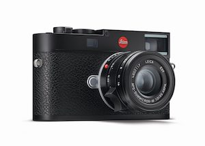
For more than a century, the name Leica has stood for lenses and cameras with the highest quality, first-class workmanship “Made in Germany” and ease of use. Whether photography beginners, ambitious amateur, or professional photographers – they all gladly rely on the high-quality high-tech products from the Leitz Park in Wetzlar (Germany), the corporate headquarters of Leica Camera AG.
With the new Leica M11, the company is once again setting a milestone, combining the unique experience of traditional rangefinder photography with state-of-the-art camera technology. At the heart of the new M generation in the iconic Leica design is a full-frame BSI CMOS sensor with triple resolution technology: raw files in DNG format or JPEGs can be created with a resolution of either 60, 36, or 18 megapixels. Thus, the M11 offers even more flexibility and allows shooting in outstanding image quality.
This is where AT&S, as a development partner of innovative PCB and interconnection technologies, comes into play: A total of twelve different AT&S circuit boards are included in the new M11, including the solutions for integrating the image sensor and image processing. “The trust that a premium manufacturer like Leica places in AT&S products and solutions once again confirms our company’s solution expertise and technological capabilities,” says AT&S CEO Andreas Gerstenmayer.
The printed circuit boards are manufactured both at the Hinterberg site and at the AT&S plant in Korea. The use of special AT&S technologies that allow very compact and flexible electronic interconnection solutions makes it possible for Leica to build digital cameras that offer maximum performance in the smallest possible space while consuming very little energy.
Share on:


Testimonial
"Advertising in PCB007 Magazine has been a great way to showcase our bare board testers to the right audience. The I-Connect007 team makes the process smooth and professional. We’re proud to be featured in such a trusted publication."
Klaus Koziol - atgSuggested Items
Nvidia’s Blackwell Chips Made in Arizona Still Head to Taiwan for Final Assembly
10/27/2025 | I-Connect007 Editorial TeamNvidia has begun production of its next-generation Blackwell GPUs in the United States, but the company still depends heavily on Taiwan to complete the process, The Register reported.
American Standard Circuits Launches 50th 77-Second Webinar
10/27/2025 | American Standard CircuitsAnaya Vardya, President and CEO of American Standard Circuits/ASC Sunstone Circuits is pleased to announce that they have recently unveiled their 50th 77-second webinar.
KYZEN Brings Reliability to Life at productronica 2025 with ANALYST² Process Control Demos
10/22/2025 | KYZEN'KYZEN, the global leader in innovative environmentally responsible cleaning chemistries, will exhibit at productronica 2025, November 18–21 in Munich, Germany, where the company will put a spotlight on its award-winning KYZEN ANALYST² process control system in Hall A4, Stand 450.
SCHMID Group Secures Major Orders for AI Server PCB Production Equipment
10/22/2025 | SCHMID GroupSCHMID Group, a global equipment maker and solution provider for Printed Circuit Boards (PCB) and IC-Substrate manufacturing – announced the successful acquisition of two significant orders in the fast-growing field of PCB for artificial intelligence (AI) server applications. So called AI-Server-Boards.
SEMICON Japan 2025 to Spotlight Sustainability in AI and Semiconductor Innovation
10/22/2025 | SEMISEMICON Japan 2025, the largest gathering of leaders from the microelectronics manufacturing supply chain in Japan, will bring together more than 1,200 exhibitors showcasing semiconductor solutions from December 17-19 at Tokyo Big Sight.