


 It’s Only Common Sense: Stay Curious, My Friends
 The Marketing Minute: AI Is Watching Your Marketing Habits
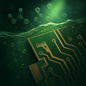
 Trouble in Your Tank: The Role of Organic Solderability Preservatives in Advanced Packaging


Atotech, a leading specialty chemicals technology company and a market leader in advanced electroplating solutions, and Schweitzer Engineering Laboratories (SEL), an industry leader in the design and manufacture of digital products and systems that protect, control, and automate electric power systems, announced that they will partner at SEL’s state-of-the-art manufacturing facility under construction in Idaho, USA.
SEL will utilize Atotech’s innovative Uniplate equipment technology in their new 162,000 square-foot facility that will serve as home for SEL’s printed circuit board manufacturing operation. The Uniplate family of equipment is the industry standard for horizontal inline printed circuit board processes, from desmear and metallization to flash copper plating. The lines are scheduled to be commissioned in 2022.
John Hendrickson, Senior Engineering Manager at SEL, who will oversee SEL’s new operation, said: “As we start manufacturing our own printed circuit boards, we are committed to building the most modern, environmentally friendly, and safe PCB manufacturing facility in the United States. Atotech is a leader in their field and the right partner for us. Their horizontal plating technology offers an easy approach to automation with a focus on reducing chemical usage. This will help us meet our water recycling goals.”
Atotech’s significant investment into environmentally sound solutions benefits customers’ products and their production processes. These solutions reduce water, chemistry, energy, and waste generation, while reducing costs and meeting customer expectations for future PCB manufacturing.
“We are very excited to work with SEL to realize their needs in Idaho,” said Harald Ahnert, President of the Electronics segment at Atotech. “The equipment selected by SEL combines years of Atotech engineering leadership for horizontal production equipment. The Uniplate® family brings a highly automated and environmentally sound approach to PCB manufacturing.”
SEL previously announced that local in-house production of the PCB’s used in their digital products will provide the company with more freedom to experiment and innovate. It will also increase supply-chain security and yield superior product quality.


