


 It’s Only Common Sense: Stay Curious, My Friends
 The Marketing Minute: AI Is Watching Your Marketing Habits
 Trouble in Your Tank: The Role of Organic Solderability Preservatives in Advanced Packaging


Averatek Corporation has announced its participation in this year’s JPCA Show Exhibition and NPI Presentation June 15th through June 17th, at the Big Sight center in Tokyo, Japan, (Booth#: 5F-21).
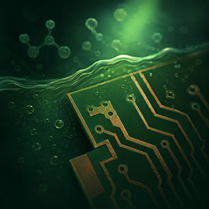
Averatek will be presenting advanced HDI PCB and package substrate manufacturing technology A-SAP™ and associated new materials ACL™ and CBF™. Averatek will also jointly present with Toyo Aluminium K.K. (“Toyo”) about a new catalyzed aluminum foil (Ranafoil™) for A-SAP™ during the show. The Averatek Semi-Additive Process (A-SAP™) and these new materials allow for filling the technical gap between mSAP HDI PCB and the package substrates - and dramatically expand material selection flexibility in package substrate manufacturing.
Averatek will first present on Friday, June 17th, at the NPI presentation. Toyo will have a presentation on the same day at the NPI presentation. Both companies will share booth #5F-21 during the show June 15th through June 17th.
The Averatek Semi-Additive Process (A-SAP™) can be used for a variety of materials with very thin electroless base copper layer - unlike other semi-additive processes (SAPs). The palladium catalyst is formed by LMI™ (Liquid Metal Ink™), which allows for less than 10 nanometer of uniform metal coating with A-SAP™.
ACL™ (Aluminum Clad Laminate) and CBF™ (Catalyzed Build-up Film) use a catalyzed aluminum foil by Toyo which provides well-controlled surface texture for the process, and very uniformly coated palladium metal. Developed for outer and build-up layers, now ACL™ and CBF™ enhance the use of A-SAP™.


