


 The Marketing Minute: Marketing With Layers
 The Right Approach: Electro-Tek—A Williams Family Legacy, Part 1
 It’s Only Common Sense: If You’re Not Differentiated, You’re Dead


TANAKA Establishes New Ruthenium Film Deposition Process
June 23, 2022 | ACN NewswireEstimated reading time: 3 minutes
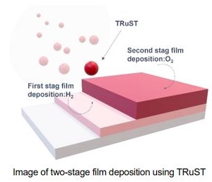
TANAKA Kikinzoku Kogyo K.K., which operates the TANAKA Precious Metals manufacturing business, announced that TANAKA has established a two-stage film deposition process using the liquid ruthenium (Ru) precursor "TRuST." TRuST is a precursor that has excellent reactivity with both oxygen and hydrogen and can form high-quality ruthenium films. This process is a two-stage atomic layer deposition (ALD) process that uses hydrogen film formation to create a thin anti-oxidation film and oxygen for the deposition of a high-quality ruthenium film. It eradicates concerns that the substrate will become oxidized and, at the same time, can prevent the drop in ruthenium purity that occurs during hydrogen film deposition.
The film deposition process was proposed by Professor Soo-Hyun Kim from the School of Materials Science and Engineering, College of Engineering, Yeungnam University in South Korea. The development and evaluation of the film deposition process were jointly conducted by Professor Kim and TANAKA Kikinzoku Kogyo.
This technology is expected to achieve greater miniaturization and improved durability of semiconductors. It can therefore be expected to be used in data centers and smartphones - which require even greater data processing capabilities - and contribute toward advanced technologies such as IoT and autonomous driving, which require sophisticated technological innovations.
Two-Stage Film Deposition Process Using Oxygen And Hydrogen
TANAKA Kikinzoku Kogyo is developing high-purity precious metal precursors “centered on ruthenium” for next-generation semiconductors. So far, single-stage film deposition using oxygen has been the mainstream process for film deposition. However, the company has now succeeded in a two-stage film deposition process using oxygen and hydrogen.
This two-stage film deposition process reduces the risk of surface oxidation of the base caused by hydrogen film deposition and allows high-purity film deposition that maintains ruthenium purity at almost 100% using oxygen film deposition. Furthermore, by forming the base first using hydrogen film deposition, the ruthenium film on top of the base created using oxygen film deposition will be smooth and dense, achieving a lower resistance than before.
Generally, specific resistivity increases when film thickness decreases, which is an issue in film deposition of semiconductors. With this new process, it was confirmed that an even lower resistance results from a two-stage film deposition that uses hydrogen in addition to oxygen film deposition, especially in the range of 10 nm and below. As semiconductors become even smaller in scale in the future, demand for thinner film deposition with low resistance is also expected for ruthenium films, and a two-stage film deposition allows this issue to be resolved. In addition, the new low-resistance, high-purity ruthenium film created by the two-stage film deposition can be achieved using the same raw materials and film deposition temperature for both stages. Therefore, film deposition is possible using the same film deposition equipment, allowing capital investment costs to be suppressed. Details will be announced at the AA2-TuA: ALD for BEOL session of the ALD 2022 conference being held in Ghent, Belgium, on June 28, 2022.
TANAKA Kikinzoku Kogyo's Liquid Ruthenium Precursor "TRuST"
In the past, the most common thin film and wiring materials used for semiconductors were copper, tungsten, and cobalt, but there are increasing expectations for the precious metal ruthenium to promote greater miniaturization of semiconductors because of its lower resistance and higher durability. Therefore, TANAKA Kikinzoku Kogyo developed TRuST - a liquid ruthenium precursor for chemical vapor deposition (CVD) and ALD that achieved the world's highest vapor pressure value - and started providing samples in 2020.
By increasing to the world's highest vapor pressure value, which is more than 100 times higher than existing precursors, this precursor raises the concentration of precursor in the film deposition chamber and the adsorption density of precursor molecules on the substrate surface, achieving excellent step coverage and improved film deposition speed.
State of the Semiconductor Industry and Background
The progress of advanced technologies such as IoT, AI, 5G, and the metaverse has led to rapidly increasing volumes of digital data used by digital devices such as smartphones. Therefore, in the development of semiconductors, the need for even greater miniaturization is increasing to enable the creation of devices with higher performance and lower energy consumption. In the aspect of durability, degradation due to base oxidation is also a major issue in semiconductor development. Furthermore, the development of electric vehicles and self-driving cars requires similar needs for the miniaturization of automotive semiconductors along with further improvement in durability.
In the semiconductor industry, which will require greater miniaturization and improved durability in the future, TANAKA Kikinzoku Kogyo seeks to further reduce costs and achieve higher quality by improving the film deposition speed of liquid ruthenium precursors. At the same time, the company will contribute to greater miniaturization and improved durability of semiconductors to support the development of new advanced technologies enabled by semiconductors.
Share on:


Testimonial
"The I-Connect007 team is outstanding—kind, responsive, and a true marketing partner. Their design team created fresh, eye-catching ads, and their editorial support polished our content to let our brand shine. Thank you all! "
Sweeney Ng - CEE PCBSuggested Items
Episode 6 of Ultra HDI Podcast Series Explores Copper-filled Microvias in Advanced PCB Design and Fabrication
10/15/2025 | I-Connect007I-Connect007 has released Episode 6 of its acclaimed On the Line with... American Standard Circuits: Ultra High Density Interconnect (UHDI) podcast series. In this episode, “Copper Filling of Vias,” host Nolan Johnson once again welcomes John Johnson, Director of Quality and Advanced Technology at American Standard Circuits, for a deep dive into the pros and cons of copper plating microvias—from both the fabricator’s and designer’s perspectives.
Nolan’s Notes: Tariffs, Technologies, and Optimization
10/01/2025 | Nolan Johnson -- Column: Nolan's NotesLast month, SMT007 Magazine spotlighted India, and boy, did we pick a good time to do so. Tariff and trade news involving India was breaking like a storm surge. The U.S. tariffs shifted India from one of the most favorable trade agreements to the least favorable. Electronics continue to be exempt for the time being, but lest you think that we’re free and clear because we manufacture electronics, steel and aluminum are specifically called out at the 50% tariff levels.
MacDermid Alpha & Graphic PLC Lead UK’s First Horizontal Electroless Copper Installation
09/30/2025 | MacDermid Alpha & Graphic PLCMacDermid Alpha Electronics Solutions, a leading supplier of integrated materials and chemistries to the electronics industry, is proud to support Graphic PLC, a Somacis company, with the installation of the first horizontal electroless copper metallization process in the UK.
Electrodeposited Copper Foils Market to Grow by $11.7 Billion Over 2025-2032
09/18/2025 | Globe NewswireThe global electrodeposited copper foils market is poised for dynamic growth, driven by the rising adoption in advanced electronics and renewable energy storage solutions.
MacDermid Alpha Showcases Advanced Interconnect Solutions at PCIM Asia 2025
09/18/2025 | MacDermid Alpha Electronics SolutionsMacDermid Alpha Electronic Solutions, a global leader in materials for power electronics and semiconductor assembly, will showcase its latest interconnect innovations in electronic interconnect materials at PCIM Asia 2025, held from September 24 to 26 at the Shanghai New International Expo Centre, Booth N5-E30